Datasheet 搜索 > 运算放大器 > TI(德州仪器) > OPA2107AP 数据手册 > OPA2107AP 数据手册 3/8 页
 器件3D模型
¥ 1.714
OPA2107AP 数据手册 - TI(德州仪器)
制造商:
TI(德州仪器)
分类:
运算放大器
封装:
PDIP-8
描述:
TEXAS INSTRUMENTS OPA2107AP 运算放大器, 双路, 4.5 MHz, 2个放大器, 18 V/µs, ± 10V 至 ± 18V, DIP, 8 引脚
Pictures:
3D模型
符号图
焊盘图
引脚图
产品图
页面导航:
封装尺寸在P8
封装信息在P1P2
技术参数、封装参数在P2
应用领域在P1
导航目录
OPA2107AP数据手册
Page:
of 8 Go
若手册格式错乱,请下载阅览PDF原文件
NOTES
1
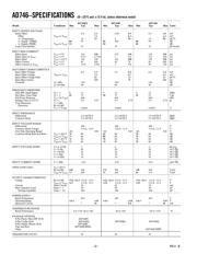
Input Offset Voltage specifications are guaranteed after 5 minutes of operation at T
A
= +25°C.
2
PSRR test conditions: +V
S
= 15 V, –V
S
= –12 V to –18 V and +V
S
= 12 V to 18 V, –V
S
= –15 V.
3
Bias Current Specifications are guaranteed maximum at either input after 5 minutes of operation at T
A
= +25°C. For higher temperature, the current doubles every
10°C.
4
Gain = –1, Rl = 2 k, Cl = 10 pF.
5
Defined as voltage between inputs, such that neither exceeds ±10 V from ground.
6
Typically exceeding –14.1 V negative common-mode voltage on either input results in an output phase reversal.
Specifications subject to change without notice.
Specifications in boldface are tested on all production units at final electrical test. Results from those tests are used to calculate outgoing quality levels. All min and
max specifications are guaranteed, although only those shown in boldface are tested on all production units.
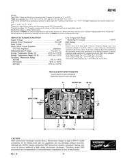
ABSOLUTE MAXIMUM RATINGS
1
Supply Voltage . . . . . . . . . . . . . . . . . . . . . . . . . . . . . . . . .±18 V
Internal Power Dissipation
2
. . . . . . . . . . . . . . . . . . . . . 500 mW
Input Voltage . . . . . . . . . . . . . . . . . . . . . . . . . . . . . . . . . . .±V
S
Output Short Circuit Duration
(For One Amplifier) . . . . . . . . . . . . . . . . . . . . . . . Indefinite
Differential Input Voltage . . . . . . . . . . . . . . . . . . +V
S
and –V
S
Storage Temperature Range (Q) . . . . . . . . . . –65°C to +150°C
Storage Temperature Range (N, R) . . . . . . . . –65°C to +125°C
Operating Temperature Range
AD746J . . . . . . . . . . . . . . . . . . . . . . . . . . . . . .0°C to +70°C
AD746A/B . . . . . . . . . . . . . . . . . . . . . . . . . . –40°C to +85°C
AD746S . . . . . . . . . . . . . . . . . . . . . . . . . . . –55°C to +125°C
Lead Temperature Range
(Soldering 60 seconds) . . . . . . . . . . . . . . . . . . . . . . . +300°C
ESD Rating . . . . . . . . . . . . . . . . . . . . . . . . . . . . . . . . . . . . . . .
NOTES
1
Stresses above those listed under “Absolute Maximum Ratings” may cause
permanent damage to the device. This is a stress rating only and functional
operation of the device at these or any other conditions above those indicated in
the operational section of this specification is not implied. Exposure to absolute
maximum rating conditions for extended periods may affect device reliability.
2
8-Pin Plastic Package: θ
JA
= 100°C/Watt, θ
JC
= 50°C/Watt
8-Pin Cerdip Package: θ
JA
= 110°C/Watt, θ
JC
= 30°C/Watt
8-Pin Small Outline Package: θ
JA
= 160°C/Watt, θ
JC
= 42°C/Watt
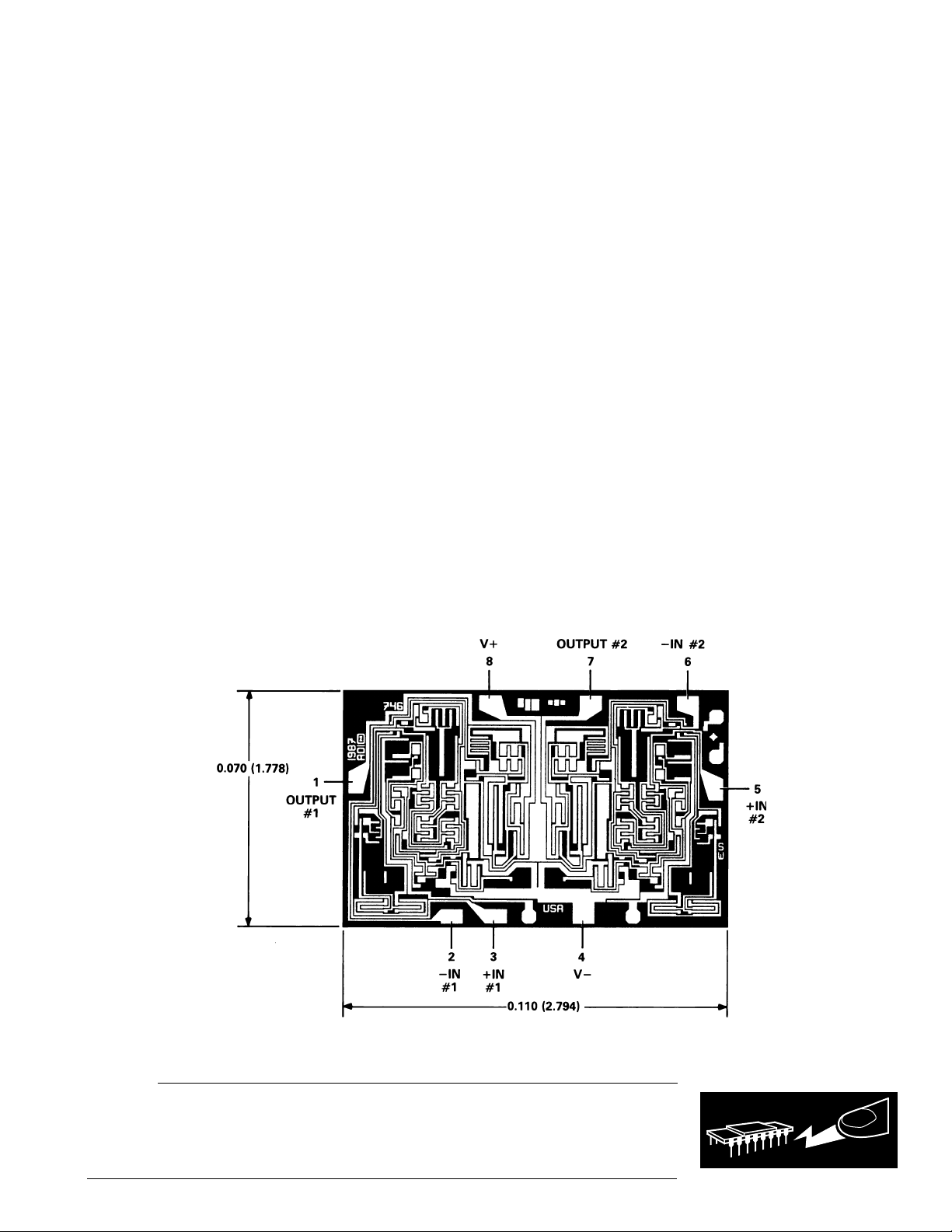
METALIZATION PHOTOGRAPH
Contact factory for latest dimensions.
Dimensions shown in inches and (mm).
WARNING!
ESD SENSITIVE DEVICE
CAUTION
ESD (electrostatic discharge) sensitive device. Electrostatic charges as high as 4000 V readily
accumulate on the human body and test equipment and can discharge without detection.
Although the AD746 features proprietary ESD protection circuitry, permanent damage may
occur on devices subjected to high energy electrostatic discharges. Therefore, proper ESD
precautions are recommended to avoid performance degradation or loss of functionality.
AD746
REV. B
–3–
器件 Datasheet 文档搜索
AiEMA 数据库涵盖高达 72,405,303 个元件的数据手册,每天更新 5,000 多个 PDF 文件
