Datasheet 搜索 > 运算放大器 > TI(德州仪器) > OPA2132UA/2K5 数据手册 > OPA2132UA/2K5 数据手册 4/30 页
 器件3D模型
¥ 18.416
OPA2132UA/2K5 数据手册 - TI(德州仪器)
制造商:
TI(德州仪器)
分类:
运算放大器
封装:
SOIC-8
描述:
OPA2132UA/2K5 编带
Pictures:
3D模型
符号图
焊盘图
引脚图
产品图
页面导航:
引脚图在P3P4Hot
典型应用电路图在P12P13
原理图在P10P12P15
封装尺寸在P18P19P20P22P23
标记信息在P18P19P20
封装信息在P17P18P19P20P21P22P23
技术参数、封装参数在P4P14
应用领域在P1P30
电气规格在P5P6
导航目录
OPA2132UA/2K5数据手册
Page:
of 30 Go
若手册格式错乱,请下载阅览PDF原文件
OPA132
,
OPA2132
,
OPA4132
SBOS054B –JANUARY 1995–REVISED SEPTEMBER 2015
www.ti.com
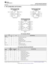
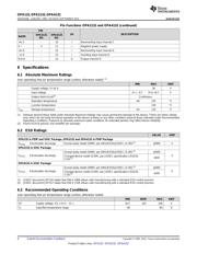
Pin Functions OPA2132 and OPA4132 (continued)
PIN
I/O DESCRIPTION
OPA2132 OPA4132
NAME
NO. NO.
+In C – 10 I Noninverting input channel C
V– 4 11 — Negative power supply
+In D – 12 I Noninverting input channel D
–In D – 13 I Inverting input channel D
Out D – 14 O Output channel D
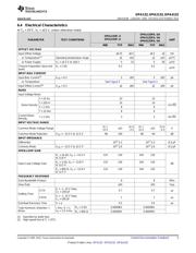
6 Specifications
6.1 Absolute Maximum Ratings
over operating free-air temperature range (unless otherwise noted)
(1)
MIN MAX UNIT
Supply voltage, V+ to V– 36 V
Input voltage (V–) –0.7 (V+) +0.7 V
Output short-circuit
(2)
Continuous
Operation temperature –40 125 °C
Junction temperature 150 °C
T
stg
Storage temperature –55 125 °C
(1) Stresses beyond those listed under Absolute Maximum Ratings may cause permanent damage to the device. These are stress ratings
only, which do not imply functional operation of the device at these or any other conditions beyond those indicated under Recommended
Operating Conditions. Exposure to absolute-maximum-rated conditions for extended periods may affect device reliability.
(2) Short-circuit to ground, one amplifier per package.
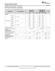
6.2 ESD Ratings
VALUE UNIT
OPA132 in PDIP and SOIC Package, OPA2132 and OPA4132 in PDIP Package
V
(ESD)
Electrostatic discharge Human-body model (HBM), per ANSI/ESDA/JEDEC JS-001
(1)
±2000 V
OPA2132 in SOIC Package
Human-body model (HBM), per ANSI/ESDA/JEDEC JS-001
(1)
±2000
V
(ESD)
Electrostatic discharge V
Charged-device model (CDM), per JEDEC specification JESD22-
±500
C101
(2)
OPA4132 in SOIC Package
Human-body model (HBM), per ANSI/ESDA/JEDEC JS-001
(1)
±2000
V
(ESD)
Electrostatic discharge V
Charged-device model (CDM), per JEDEC specification JESD22-
±200
C101
(2)
(1) JEDEC document JEP155 states that 500-V HBM allows safe manufacturing with a standard ESD control process.
(2) JEDEC document JEP157 states that 250-V CDM allows safe manufacturing with a standard ESD control process.
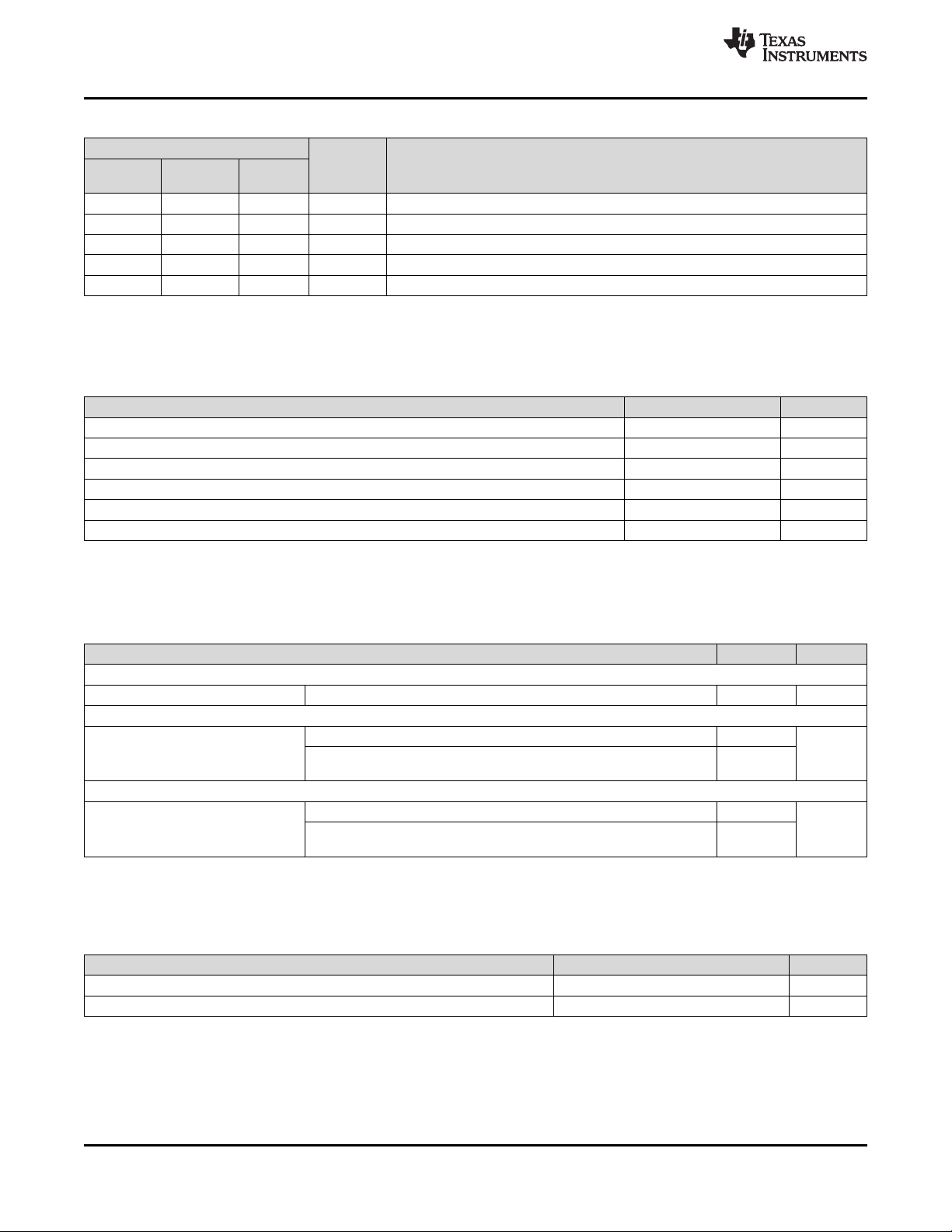
6.3 Recommended Operating Conditions
over operating free-air temperature range (unless otherwise noted)
MIN NOM MAX UNIT
VS Supply voltage, VS = (V+) – (V–) ±2.5 ±15 ±18 V
T
A
Specified temperature range –40 85 °C
4 Submit Documentation Feedback Copyright © 1995–2015, Texas Instruments Incorporated
Product Folder Links: OPA132 OPA2132 OPA4132
器件 Datasheet 文档搜索
AiEMA 数据库涵盖高达 72,405,303 个元件的数据手册,每天更新 5,000 多个 PDF 文件
