Datasheet 搜索 > 运算放大器 > TI(德州仪器) > OPA2277U 数据手册 > OPA2277U 数据手册 27/45 页
 器件3D模型
¥ 15.939
OPA2277U 数据手册 - TI(德州仪器)
制造商:
TI(德州仪器)
分类:
运算放大器
封装:
SOIC-8
描述:
TEXAS INSTRUMENTS OPA2277U 运算放大器, 双路, 1 MHz, 2个放大器, 0.8 V/µs, ± 2V 至 ± 18V, ± 5V 至 ± 15V, SOIC, 8 引脚
Pictures:
3D模型
符号图
焊盘图
引脚图
产品图
页面导航:
引脚图在P3P4Hot
典型应用电路图在P26P27P28
原理图在P16P23P26P30
封装尺寸在P33P34P35P36P38P39
标记信息在P33P34P35P36P37
封装信息在P32P33P34P35P36P37P38P39
技术参数、封装参数在P5P16P29
应用领域在P1P16P22P24P37P45
电气规格在P7P8P9P29
导航目录
OPA2277U数据手册
Page:
of 45 Go
若手册格式错乱,请下载阅览PDF原文件
400ns/div
5mV/div
OPA228
400ns/div
5mV/div
OPA228
1kΩ 2kΩ
15pF
OPA228
2kΩ
100pF
2kΩ
OPA228
22pF
2kΩ
100pF
2kΩ
OPA227
,
OPA2227
,
OPA4227
OPA228
,
OPA2228
,
OPA4228
www.ti.com
SBOS110B –MAY 1998–REVISED JUNE 2015
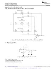
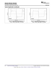
Typical Application (continued)
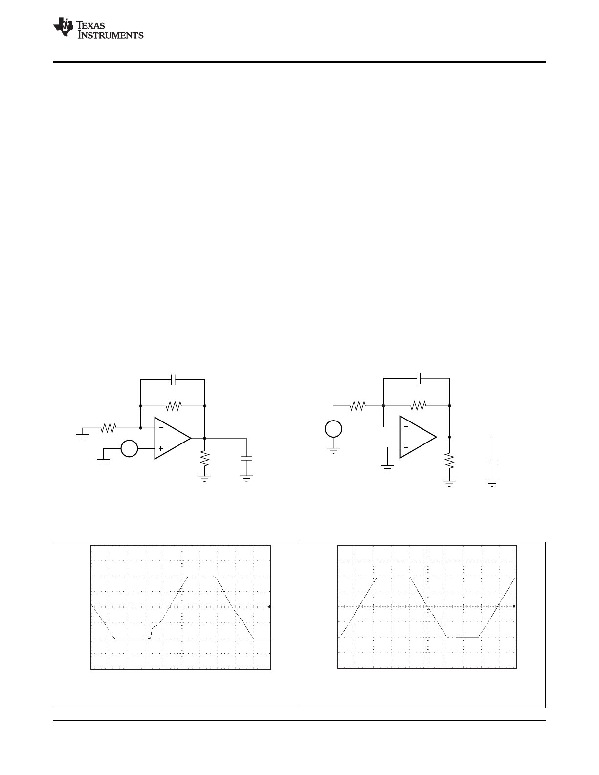
8.2.2 Detailed Design Procedure
8.2.2.1 Using the OPAx228 in Low Gains
The OPAx228 family is intended for applications with signal gains of 5 or greater, but it is possible to take
advantage of their high-speed in lower gains. Without external compensation, the OPA228 has sufficient phase
margin to maintain stability in unity gain with purely resistive loads. However, the addition of load capacitance
can reduce the phase margin and destabilize the operational amplifier.
A variety of compensation techniques have been evaluated specifically for use with the OPA228. The
recommended configuration consists of an additional capacitor (C
F
) in parallel with the feedback resistance, as
shown in Figure 51 and Figure 52. This feedback capacitor serves two purposes in compensating the circuit. The
operational amplifier’s input capacitance and the feedback resistors interact to cause phase shift that can result
in instability. C
F
compensates the input capacitance, minimizing peaking. Additionally, at high frequencies, the
closed-loop gain of the amplifier is strongly influenced by the ratio of the input capacitance and the feedback
capacitor. Thus, C
F
can be selected to yield good stability while maintaining high-speed.
Without external compensation, the noise specification of the OPA228 is the same as that for the OPA227 in
gains of 5 or greater. With the additional external compensation, the output noise of the of the OPA228 will be
higher. The amount of noise increase is directly related to the increase in high-frequency closed-loop gain
established by the C
IN
/C
F
ratio.
Figure 51 and Figure 52 show the recommended circuit for gains of 2 and –2, respectively. The figures suggest
approximate values for C
F
. Because compensation is highly dependent on circuit design, board layout, and load
conditions, C
F
should be optimized experimentally for best results. Figure 53 and Figure 55 show the large- and
small-signal step responses for the G = 2 configuration with 100-pF load capacitance.Figure 54 and Figure 56
show the large- and small-signal step responses for the G = –2 configuration with 100-pF load capacitance.
Figure 51. Compensation of the OPA228 for G = 2 Figure 52. Compensation for OPA228 for G = –2
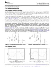
8.2.3 Application Curves
Figure 54. Large-Signal Step Response, G = –2, CLOAD =
Figure 53. Large-Signal Step Response, G = 2,
100 pF, Input Signal = 5 Vp-p
C
LOAD
= 100 pF, Input Signal = 5 Vp-p
Copyright © 1998–2015, Texas Instruments Incorporated Submit Documentation Feedback 27
Product Folder Links: OPA227 OPA2227 OPA4227 OPA228 OPA2228 OPA4228
器件 Datasheet 文档搜索
AiEMA 数据库涵盖高达 72,405,303 个元件的数据手册,每天更新 5,000 多个 PDF 文件
