Datasheet 搜索 > 视频放大器 > TI(德州仪器) > OPA3693IDBQR 数据手册 > OPA3693IDBQR 数据手册 5/34 页
 器件3D模型
¥ 25.28
OPA3693IDBQR 数据手册 - TI(德州仪器)
制造商:
TI(德州仪器)
分类:
视频放大器
封装:
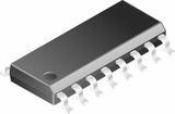
SSOP-16
描述:
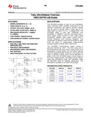
具有禁用功能的三路、超宽带、固定增益、视频缓冲器 16-SSOP
Pictures:
3D模型
符号图
焊盘图
引脚图
产品图
页面导航:
封装尺寸在P28P30P31
标记信息在P28
封装信息在P28P29P30P31
应用领域在P34
导航目录
OPA3693IDBQR数据手册
Page:
of 34 Go
若手册格式错乱,请下载阅览PDF原文件
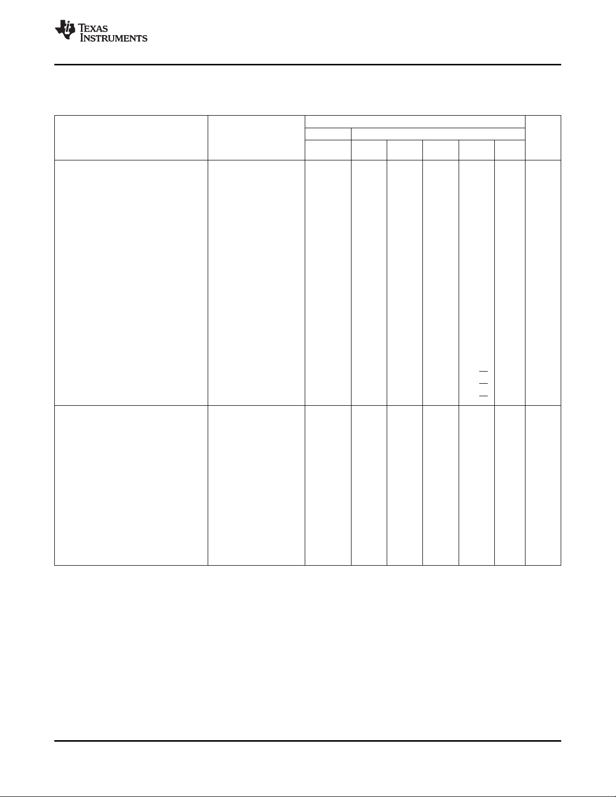
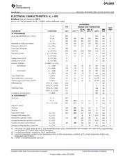
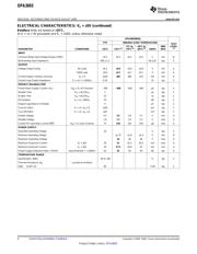
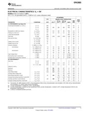
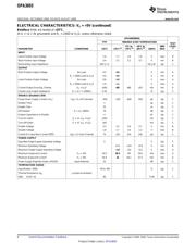
ELECTRICAL CHARACTERISTICS: V
S
= +5V
OPA3693
www.ti.com
............................................................................................................................................ SBOS353A – DECEMBER 2006 – REVISED AUGUST 2008
Boldface limits are tested at +25 ° C.
At G = +2 ( – IN grounded) and R
L
= 100 Ω to V
S
/2, unless otherwise noted.
OPA3693IDBQ
TYP MIN/MAX OVER TEMPERATURE
TEST
0 ° C to – 40 ° C to MIN/ LEVEL
PARAMETER CONDITIONS +25 ° C +25 ° C
(2)
+70 ° C
(3)
+85 ° C
(3)
UNITS MAX
(1)
AC PERFORMANCE (see Figure 29)
Small-Signal Bandwidth (V
O
= 0.5V
PP
) G = +1 600 MHz typ C
G = +2 500 400 390 380 MHz min B
G = – 1 450 C
Bandwidth for 0.2dB Gain Flatness V
O
< 0.5V
PP
280 110 100 96 MHz min B
Peaking at a Gain of +1 V
O
< 0.5V
PP
2.2 2.9 3.9 4.2 dB max B
Large-Signal Bandwidth V
O
= 2V
PP
425 MHz typ C
Slew Rate 2V Step 1500 1200 1100 1000 V/ µ s min B
Rise-and-Fall Time V
O
= 0.5V Step 0.8 ns typ C
V
O
= 2V Step 1.0 ns typ C
Settling Time to 0.02% V
O
= 2V Step 16 ns typ C
Settling Time to 0.1% V
O
= 2V Step 12 ns typ C
Harmonic Distortion f = 10MHz, V
O
= 2V
PP
2nd-Harmonic R
L
= 100 Ω to V
S
/2 – 72 – 62 – 62 – 61 dBc max B
R
L
≥ 500 Ω to V
S
/2 – 73 – 67 – 66 – 66 dBc max B
3rd-Harmonic R
L
= 100 Ω to V
S
/2 – 67 – 62 – 61 – 60 dBc max B
R
L
≥ 500 Ω to V
S
/2 – 67 – 62 – 61 – 60 dBc max B
Input Voltage Noise f > 1MHz 1.8 2 2.7 2.9 nV/ √ Hz max B
Noninverting Input Current Noise f > 1MHz 18 19 21 22 pA/ √ Hz max B
Inverting Input Current Noise (internal) f > 1MHz 22 24 26 27 pA/ √ Hz max B
DC PERFORMANCE
(4)
Gain Error G = +1 ± 0.8 % typ C
G = +2 ± 0.6 ± 1.2 ± 1.3 ± 1.4 % max A
G = – 1, R
s
= 0 Ω ± 0.5 ± 1.1 ± 1.2 ± 1.3 % max B
Internal R
F
and R
G
Maximum 300 341 345 347 Ω max A
Minimum 300 264 260 258 Ω min A
Input Offset Voltage V
CM
= V
S
/2 ± 0.6 ± 3.5 ± 4.0 ± 4.2 mV max A
Average Offset Voltage Drift V
CM
= V
S
/2 ± 12 ± 12 µ V/ ° C max B
Noninverting Input Bias Current V
CM
= V
S
/2 ± 5 ± 25 ± 33 ± 35 µ A max A
Average Noninverting Input Bias Current Drift V
CM
= V
S
/2 ± 170 ± 170 nA/ ° C max B
Inverting Input Bias Current (internal) V
CM
= V
S
/2 ± 20 ± 50 ± 52 ± 54 µ A max A
Average Inverting Input Bias Current Drift V
CM
= V
S
/2 ± 50 ± 60 nA/ ° C max B
(1) Test levels: (A) 100% tested at +25 ° C. Over temperature limits set by characterization and simulation. (B) Limits set by characterization
and simulation. (C) Typical value only for information.
(2) Junction temperature = ambient for +25 ° C specifications.
(3) Junction temperature = ambient at low temperature limits; junction temperature = ambient +14 ° C at high temperature limit for over
temperature specifications.
(4) Current is considered positive out of pin.
Copyright © 2006 – 2008, Texas Instruments Incorporated Submit Documentation Feedback 5
Product Folder Link(s): OPA3693
器件 Datasheet 文档搜索
AiEMA 数据库涵盖高达 72,405,303 个元件的数据手册,每天更新 5,000 多个 PDF 文件
