Datasheet 搜索 > 运算放大器 > TI(德州仪器) > OPA4277UA 数据手册 > OPA4277UA 数据手册 23/42 页
 器件3D模型
¥ 55.354
OPA4277UA 数据手册 - TI(德州仪器)
制造商:
TI(德州仪器)
分类:
运算放大器
封装:
SOIC-14
描述:
TEXAS INSTRUMENTS OPA4277UA 运算放大器, 四路, 1 MHz, 4个放大器, 0.8 V/µs, ± 2V 至 ± 18V, SOIC, 14 引脚
Pictures:
3D模型
符号图
焊盘图
引脚图
产品图
页面导航:
引脚图在P3P4P5Hot
典型应用电路图在P20P21P22
原理图在P16P19P23
封装尺寸在P27P28P29P31P32
标记信息在P27P28P29
封装信息在P26P27P28P29P30P31P32
技术参数、封装参数在P6P7P9P22
应用领域在P1P16P19P20P21P22P30P42
电气规格在P7P8P9P10P11
导航目录
OPA4277UA数据手册
Page:
of 42 Go
若手册格式错乱,请下载阅览PDF原文件
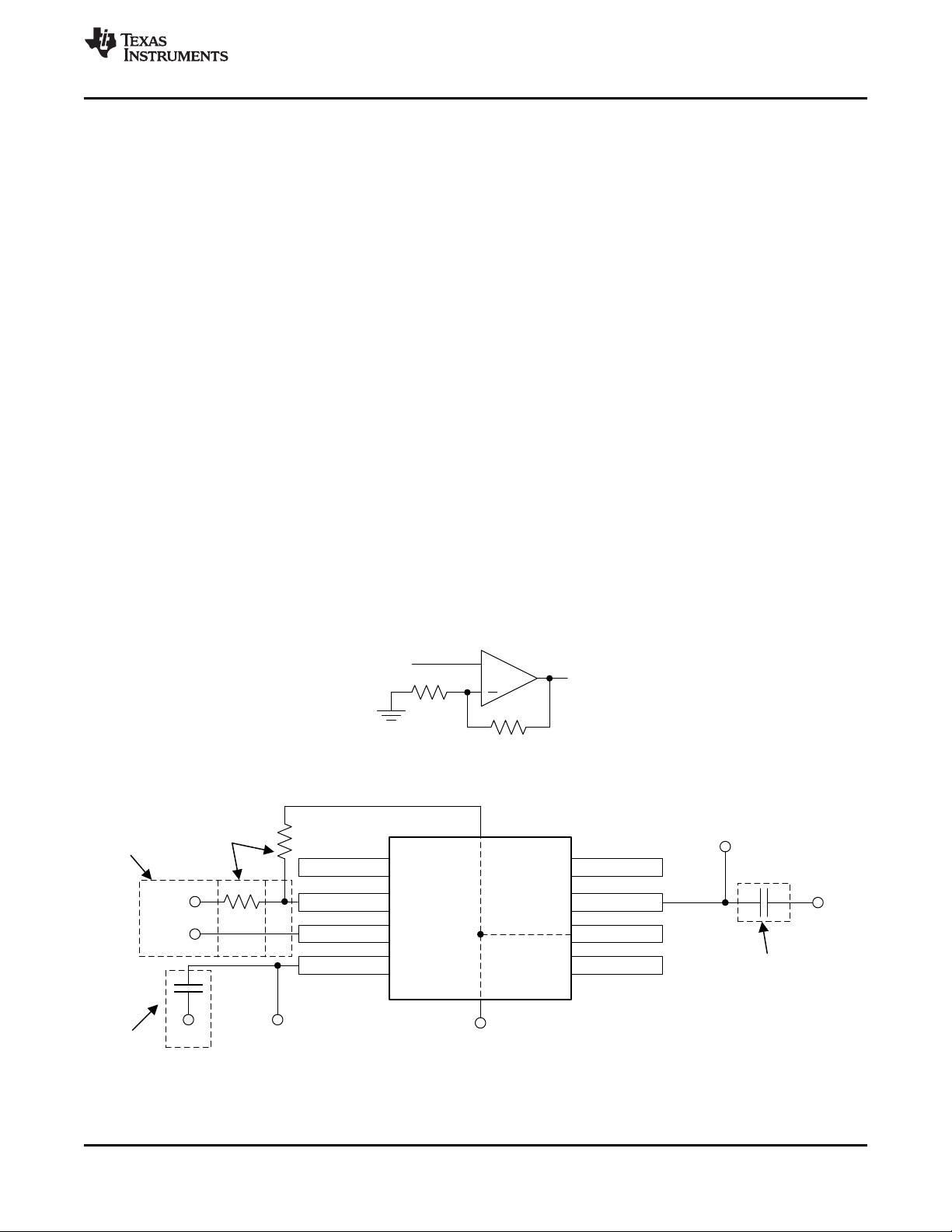
Offset trim
±IN
+IN
V±
V+
OUTPUT
NC
Offset trim
VS+
GND
VS±
GND
Ground (GND) plane on another layer
VOUT
VIN
GND
Run the input traces
as far away from
the supply lines
as possible
Use low-ESR, ceramic
bypass capacitor
RF
RG
Place components
close to device and to
each other to reduce
parasitic errors
+
VIN
VOUT
RG
RF
(Schematic Representation)
Use low-ESR,
ceramic bypass
capacitor
OPA277
,
OPA2277
,
OPA4277
www.ti.com
SBOS079B –MARCH 1999–REVISED JUNE 2015
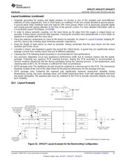
Layout Guidelines (continued)
• Separate grounding for analog and digital portions of circuitry is one of the simplest and most-effective
methods of noise suppression. One or more layers on multilayer PCBs are usually devoted to ground planes.
A ground plane helps distribute heat and reduces EMI noise pickup. Make sure to physically separate digital
and analog grounds paying attention to the flow of the ground current. For more detailed information refer to
Circuit Board Layout Techniques, SLOA089.
• In order to reduce parasitic coupling, run the input traces as far away from the supply or output traces as
possible. If these traces cannot be kept separate, crossing the sensitive trace perpendicular is much better as
opposed to in parallel with the noisy trace.
• Place the external components as close to the device as possible. As shown in Layout Example, keeping RF
and RG close to the inverting input minimizes parasitic capacitance.
• Keep the length of input traces as short as possible. Always remember that the input traces are the most
sensitive part of the circuit.
• Consider a driven, low-impedance guard ring around the critical traces. A guard ring can significantly reduce
leakage currents from nearby traces that are at different potentials.
• Cleaning the PCB following board assembly is recommended for best performance.
• Any precision integrated circuit may experience performance shifts due to moisture ingress into the plastic
package. Following any aqueous PCB cleaning process, baking the PCB assembly is recommended to
remove moisture introduced into the device packaging during the cleaning process. A low temperature, post
cleaning bake at 85°C for 30 minutes is sufficient for most circumstances.
• (DFN package only) The leadframe die pad should be soldered to a thermal pad on the PCB. The mechanical
drawings located at the end of this data sheet list the physical dimensions for the package and pad.
• (DFN package only) Soldering the exposed pad significantly improves board-level reliability during
temperature cycling, key push, package shear, and similar board-level tests. Even with applications that have
low-power dissipation, the exposed pad must be soldered to the PCB to provide structural integrity and long
term reliability.
10.2 Layout Example
Figure 33. OPA277 Layout Example for the Noninverting Configuration
Copyright © 1999–2015, Texas Instruments Incorporated Submit Documentation Feedback 23
Product Folder Links: OPA277 OPA2277 OPA4277
器件 Datasheet 文档搜索
AiEMA 数据库涵盖高达 72,405,303 个元件的数据手册,每天更新 5,000 多个 PDF 文件
