Datasheet 搜索 > TI(德州仪器) > OPA620SG 数据手册 > OPA620SG 数据手册 2/15 页


¥ 23.745
OPA620SG 数据手册 - TI(德州仪器)
制造商:
TI(德州仪器)
Pictures:
3D模型
符号图
焊盘图
引脚图
产品图
OPA620SG数据手册
Page:
of 15 Go
若手册格式错乱,请下载阅览PDF原文件
®
OPA620
2
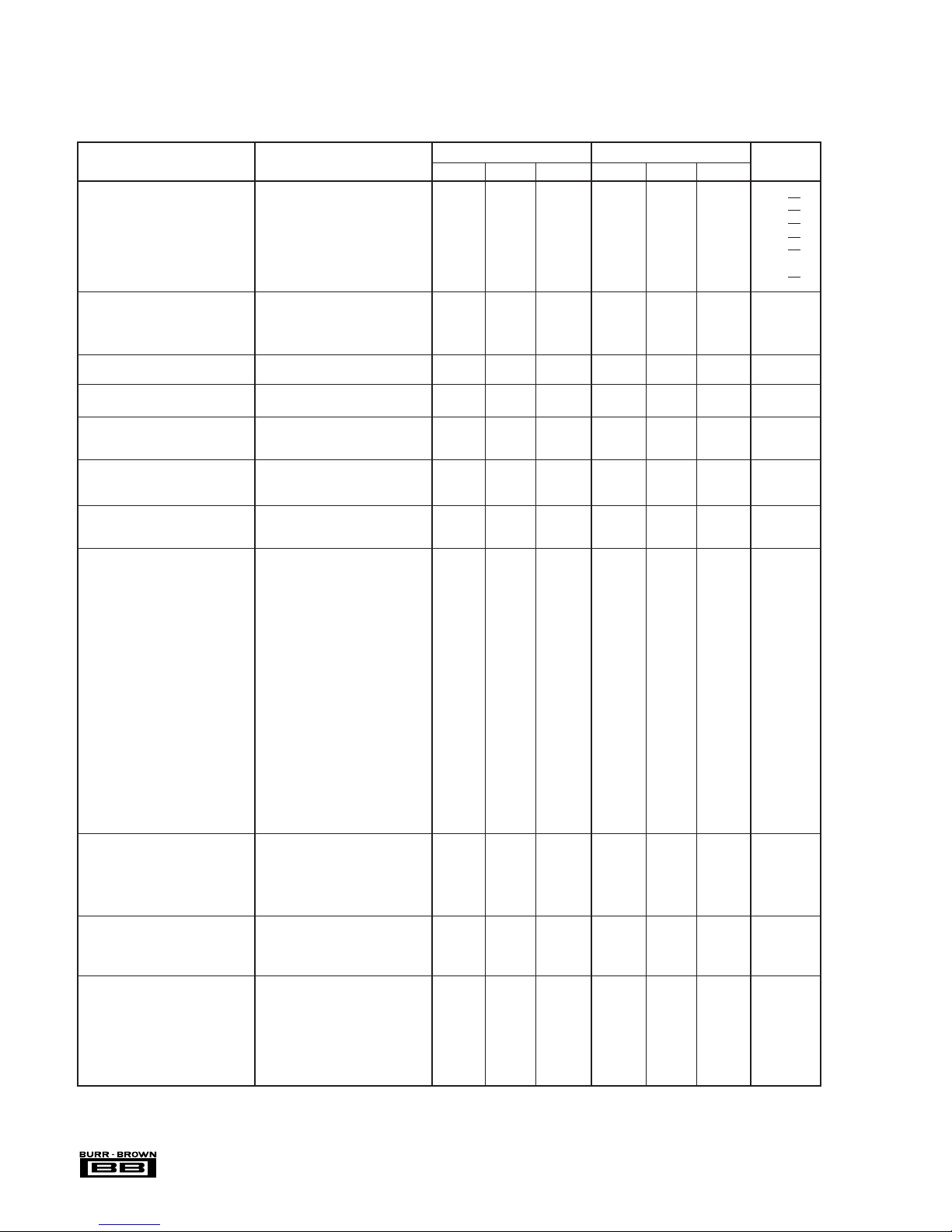
OPA620KP, KU OPA620SG
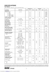
PARAMETER CONDITIONS MIN TYP MAX MIN TYP MAX UNITS
INPUT NOISE
Voltage: f
O
= 100Hz R
S
= 0Ω 10 ✻ nV/√Hz
f
O
= 1kHz 5.5 ✻ nV/√Hz
f
O
= 10kHz 3.3 ✻ nV/√Hz
f
O
= 100kHz 2.5 ✻ nV/√Hz
f
O
= 1MHz to 100MHz 2.3 ✻ nV/√Hz
f
B
= 100Hz to 10MHz 8.0 ✻ µVrms
Current: f
O
= 10kHz to 100MHz 2.3 ✻ pA/√Hz
OFFSET VOLTAGE
(1)
Input Offset Voltage V
CM
= 0VDC ±200 ±1000 ✻✻ µV
Average Drift T
A
= T
MIN
to T
MAX
±8 ✻ µV/°C
Supply Rejection ±V
CC
= 4.5V to 5.5V 50 60 ✻✻ dB
BIAS CURRENT
Input Bias Current V
CM
= 0VDC 15 30 ✻✻ µA
OFFSET CURRENT
Input Offset Current V
CM
= 0VDC 0.2 2 ✻✻ µA
INPUT IMPEDANCE
Differential Open-Loop 15 ||
1 ✻ kΩ ||
pF
Common-Mode 1 ||
1 ✻ MΩ ||
pF
INPUT VOLTAGE RANGE
Common-Mode Input Range ±3.0 ±3.5 ✻✻ V
Common-Mode Rejection V
IN
= ±2.5VDC, V
O
= 0VDC 65 75 ✻✻ dB
OPEN-LOOP GAIN, DC
Open-Loop Voltage Gain R
L
= 100Ω 50 60 ✻✻ dB
R
L
= 50Ω 48 58 ✻✻ dB
FREQUENCY RESPONSE
Closed-Loop Bandwidth Gain = +1V/V 300 ✻ MHz
(–3dB) Gain = +2V/V 100 ✻ MHz
Gain = +5V/V 40 ✻ MHz
Gain = +10V/V 20 ✻ MHz
Gain-Bandwidth Product Gain ≥ +5V/V 200 ✻ MHz
Differential Gain 3.58MHz, G = +1V/V 0.05 ✻ %
Differential Phase 3.58MHz, G = +1V/V 0.05 ✻ Degrees
Harmonic Distortion
(2)
G = +2V/V, f = 10MHz, V
O
= 2Vp-p
Second Harmonic –61 –50 ✻✻dBc
(3)
Third Harmonic –65 –55 ✻✻ dBc
Full Power Bandwidth
(2)
V
O
= 5Vp-p, Gain = +1V/V 11 16 ✻✻ MHz
V
O
= 2Vp-p, Gain = +1V/V 27 40 ✻✻ MHz
Slew Rate
(2)
2V Step, Gain = –1V/V 175 250 ✻✻ V/µs
Overshoot 2V Step, Gain = –1V/V 10 ✻ %
Settling Time: 0.1% 2V Step, Gain = –1V/V 13 ✻ ns
0.01% 25 ✻ ns
Phase Margin Gain = +1V/V 60 ✻ Degrees
Rise Time Gain = +1V/V, 10% to 90%
V
O
= 100mVp-p; Small Signal 2 ✻ ns
V
O
= 6Vp-p; Large Signal 22 ✻ ns
RATED OUTPUT
Voltage Output R
L
= 100Ω±3.0 ±3.5 ✻✻ V
R
L
= 50Ω±2.5 ±3.0 ✻✻ V
Output Resistance 1MHz, Gain = +1V/V 0.015 ✻ Ω
Load Capacitance Stability Gain = +1V/V 20 ✻ pF
Short Circuit Current Continuous ±150 ✻ mA
POWER SUPPLY
Rated Voltage ±V
CC
5 ✻ VDC
Derated Performance ±V
CC
4.0 6.0 ✻✻VDC
Current, Quiescent I
O
= 0mA 21 23 ✻✻ mA
TEMPERATURE RANGE
Specification: KP, KU Ambient Temperature –40 +85 ✻✻°C
SG –55 +125 °C
Operating: SG Ambient Temperature –55 +125 °C
KP, KU –40 +85 °C
θ
JA
:SG 125 °C/W
KP 90 °C/W
KU 100 °C/W
ELECTRICAL
At V
CC
= ±5VDC, R
L
= 100Ω, and T
A
= +25°C, unless otherwise noted.
SPECIFICATIONS
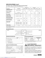
The information provided herein is believed to be reliable; however, BURR-BROWN assumes no responsibility for inaccuracies or omissions. BURR-BROWN assumes no responsibility
for the use of this information, and all use of such information shall be entirely at the user’s own risk. Prices and specifications are subject to change without notice. No patent rights or
licenses to any of the circuits described herein are implied or granted to any third party. BURR-BROWN does not authorize or warrant any BURR-BROWN product for use in life support
devices and/or systems.
Downloaded from Elcodis.com electronic components distributor
器件 Datasheet 文档搜索
AiEMA 数据库涵盖高达 72,405,303 个元件的数据手册,每天更新 5,000 多个 PDF 文件
