Datasheet 搜索 > TVS二极管 > Littelfuse(力特) > P6KE18 数据手册 > P6KE18 数据手册 1/6 页
 器件3D模型
¥ 0.922
P6KE18 数据手册 - Littelfuse(力特)
制造商:
Littelfuse(力特)
分类:
TVS二极管
封装:
DO-204AC-2
描述:
硅雪崩二极管 - 硅雪崩二极管 Silicon Avalanche Diodes - Silicon Avalanche Diodes
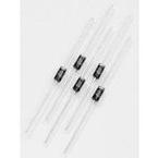
Pictures:
3D模型
符号图
焊盘图
引脚图
产品图
页面导航:
导航目录
P6KE18数据手册
Page:
of 6 Go
若手册格式错乱,请下载阅览PDF原文件
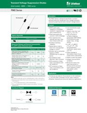
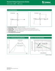
Transient Voltage Suppression Diodes
© 2015 Littelfuse, Inc.
Specifications are subject to change without notice.
Revised: 11/20/15
Axial Leaded – 600W > P6KE series
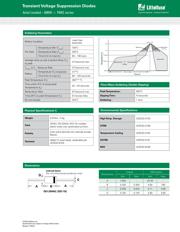
AGENCY AGENCY FILE NUMBER
E230531
TVS devices are ideal for the protection of I/O interfaces,
V
CC
bus and other vulnerable circuits used in telecom,
computer, industrial and consumer electronic applications.
Applications
Features
The P6KE Series is designed specifically to protect
sensitive electronic equipment from voltage transients
induced by lightning and other transient voltage events.
Description
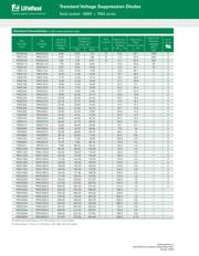
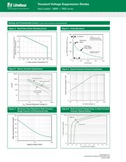
Parameter Symbol Value Unit
Peak Pulse Power Dissipation by
10/1000μs Test Waveform (Fig.2)
(Note 1), (Note 4)
P
PPM
600 W
Steady State Power Dissipation on
Infinite Heat Sink at T
L
=75ºC
P
D
5.0 W
Peak Forward Surge Current, 8.3ms
Single Half Sine Wave Unidirectional
Only (Note 2)
I
FSM
100 A
Maximum Instantaneous Forward
Voltage at 50A for Unidirectional
Only (Note 3)
V
F
3.5/5.0 V
Operating Junction and Storage
Temperature Range
T
J
, T
STG
-55 to 175 °C
Typical Thermal Resistance
Junction to Lead
R
θJL
20
°C/W
Typical Thermal Resistance
Junction to Ambient
R
θJA
75
°C/W
Notes:
1. Non-repetitive current pulse , per Fig. 4 and derated above T
J
(initial) = 25
O
C per Fig. 3.
2. Measured on 8.3ms single half sine wave or equivalent square wave, duty cycle=4 per
minute maximum.
3. V
F
< 3.5V for single die parts and V
F
< 5.0V for stacked-die parts.
4. The P
PPM
of stacked-die parts is 800W and please contact littelfuse for the detail
stacked-die parts.
Maximum Ratings and Thermal Characteristics
(T
A
=25
O
C unless otherwise noted)
Agency Approvals
• 600W peak pulse
capability at 10/1000μs
waveform, repetition rate
(duty cycles):0.01%
• Glass passivated chip
junction in DO-15 Package
• Fast response time:
typically less than 1.0ps
from 0 Volts to BV min
• Excellent clamping
capability
• Typical failure mode is
short from over-specified
voltage or current
• Whisker test is conducted
based on JEDEC
JESD201A per its table 4a
and 4c
• IEC-61000-4-2 ESD
30kV(Air), 30kV (Contact)
• ESD protection of data
lines in accordance with
IEC 61000-4-2
• EFT protection of data
lines in accordance with
IEC 61000-4-4
• Low incremental surge
resistance
• Typical I
R
less than 1μA
when V
BR
min>12V
• High temperature
to reflow soldering
guaranteed: 260°C/40sec
/ 0.375”,(9.5mm) lead
length, 5 lbs., (2.3kg)
tension
• V
BR
@ T
J
= V
BR
@25°C
x (1+
αT x (T
J
- 25))
(
αT:Temperature
Coefficient, typical value
is 0.1%)
• Plastic package is
flammability rated V-0 per
Underwriters Laboratories
• Matte tin lead–free plated
• Halogen free and RoHS
compliant
• Pb-free E3 means 2nd
level interconnect is
Pb-free and the terminal
finish material is tin(Sn)
(IPC/JEDEC J-STD-
609A.01)
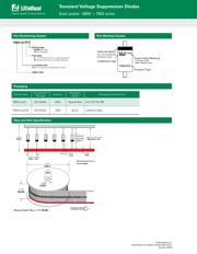
P6KE Series
Functional Diagram
Bi-directional
Uni-directional
Cathode
Anode
Bi-directional
Uni-directional
RoHS
Pb
e3
Datasheet
Additional Infomarion
Resources
Samples
器件 Datasheet 文档搜索
AiEMA 数据库涵盖高达 72,405,303 个元件的数据手册,每天更新 5,000 多个 PDF 文件
