Datasheet 搜索 > 多工器 > TI(德州仪器) > PCA9546APWT 数据手册 > PCA9546APWT 数据手册 4/38 页
 器件3D模型
¥ 8.644
PCA9546APWT 数据手册 - TI(德州仪器)
制造商:
TI(德州仪器)
分类:
多工器
封装:
TSSOP-16
描述:
TEXAS INSTRUMENTS PCA9546APWT 芯片, 开关, 4通道, I?C/SMBUS
Pictures:
3D模型
符号图
焊盘图
引脚图
产品图
页面导航:
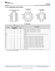
引脚图在P3Hot
典型应用电路图在P15P16P17P18
原理图在P10P16
封装尺寸在P21P22P24P25
标记信息在P21P22
封装信息在P20P21P22P23P24P25
技术参数、封装参数在P4
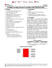
应用领域在P1P15P38
电气规格在P5P17
导航目录
PCA9546APWT数据手册
Page:
of 38 Go
若手册格式错乱,请下载阅览PDF原文件
4
PCA9546A
SCPS148G –OCTOBER 2005–REVISED MAY 2016
www.ti.com
Product Folder Links: PCA9546A
Submit Documentation Feedback Copyright © 2005–2016, Texas Instruments Incorporated
(1) Stresses beyond those listed under Absolute Maximum Ratings may cause permanent damage to the device. These are stress ratings
only, which do not imply functional operation of the device at these or any other conditions beyond those indicated under Recommended
Operating Conditions. Exposure to absolute-maximum-rated conditions for extended periods may affect device reliability.
(2) The input negative-voltage and output voltage ratings may be exceeded if the input and output current ratings are observed.
(3) The package thermal impedance is calculated in accordance with JESD 51-7.
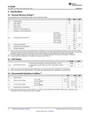
6 Specifications
6.1 Absolute Maximum Ratings
(1)
over operating free-air temperature range (unless otherwise noted)
MIN MAX UNIT
V
CC
Supply voltage –0.5 7 V
V
I
Input voltage
(2)
–0.5 7 V
I
I
Input current ±20 mA
I
O
Output current ±25 mA
Continuous current through V
CC
±100 mA
Continuous current through GND ±100 mA
θ
JA
Package thermal impedance
(3)
D package 73
°C/W
DGV package 120
DW package 57
PW package 108
RGV package 51.38
RGY package 50
P
tot
Total power dissipation 400 mW
T
A
Operating free-air temperature –40 85 °C
T
stg
Storage temperature –65 150
(1) JEDEC document JEP155 states that 500-V HBM allows safe manufacturing with a standard ESD control process.
(2) JEDEC document JEP157 states that 250-V CDM allows safe manufacturing with a standard ESD control process.
6.2 ESD Ratings
VALUE UNIT
V
(ESD)
Electrostatic discharge
Human-body model (HBM), per ANSI/ESDA/JEDEC JS-001
(1)
±2000
V
Charged-device model (CDM), per JEDEC specification JESD22-
C101
(2)
±1000
(1) All unused inputs of the device must be held at V
CC
or GND to ensure proper device operation. Refer to the TI application report,
Implications of Slow or Floating CMOS Inputs, SCBA004.
6.3 Recommended Operating Conditions
(1)
MIN MAX UNIT
V
CC
Supply voltage 2.3 5.5 V
V
IH
High-level input voltage
SCL, SDA 0.7 × V
CC
6
V
A2–A0, RESET 0.7 × V
CC
V
CC
+ 0.5
V
IL
Low-level input voltage
SCL, SDA –0.5 0.3 × V
CC
V
A2–A0, RESET –0.5 0.3 × V
CC
T
A
Operating free-air temperature –40 85 °C
器件 Datasheet 文档搜索
AiEMA 数据库涵盖高达 72,405,303 个元件的数据手册,每天更新 5,000 多个 PDF 文件
