Datasheet 搜索 > 接口芯片 > NXP(恩智浦) > PCF8591T,118 数据手册 > PCF8591T,118 数据手册 1/31 页

 器件3D模型
¥ 0
PCF8591T,118 数据手册 - NXP(恩智浦)
制造商:
NXP(恩智浦)
分类:
接口芯片
封装:
SO-16
Pictures:
3D模型
符号图
焊盘图
引脚图
产品图
页面导航:
导航目录
PCF8591T,118数据手册
Page:
of 31 Go
若手册格式错乱,请下载阅览PDF原文件

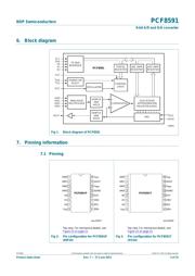
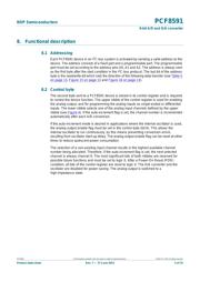
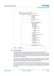
1. General description
The PCF8591 is a single-chip, single-supply low-power 8-bit CMOS data acquisition
device with four analog inputs, one analog output and a serial I
2
C-bus interface. Three
address pins A0, A1 and A2 are used for programming the hardware address, allowing
the use of up to eight devices connected to the I
2
C-bus without additional hardware.
Address, control and data to and from the device are transferred serially via the two-line
bidirectional I
2
C-bus.
The functions of the device include analog input multiplexing, on-chip track and hold
function, 8-bit analog-to-digital conversion and an 8-bit digital-to-analog conversion. The
maximum conversion rate is given by the maximum speed of the I
2
C-bus.
2. Features and benefits
Single power supply
Operating supply voltage 2.5 V to 6.0 V
Low standby current
Serial input and output via I
2
C-bus
I
2
C address selection by 3 hardware address pins
Max sampling rate given by I
2
C-bus speed
4 analog inputs configurable as single ended or differential inputs
Auto-incremented channel selection
Analog voltage range from V
SS
to V
DD
On-chip track and hold circuit
8-bit successive approximation A/D conversion
Multiplying DAC with one analog output.
3. Applications
Supply monitoring
Reference setting
Analog control loops
PCF8591
8-bit A/D and D/A converter
Rev. 7 — 27 June 2013 Product data sheet
器件 Datasheet 文档搜索
AiEMA 数据库涵盖高达 72,405,303 个元件的数据手册,每天更新 5,000 多个 PDF 文件
