Datasheet 搜索 > 时钟缓冲器、驱动器、锁相环 > Pericom Semiconductor(百利通) > PI6C10804WE 数据手册 > PI6C10804WE 数据手册 4/7 页
 器件3D模型
¥ 3.85
PI6C10804WE 数据手册 - Pericom Semiconductor(百利通)
制造商:
Pericom Semiconductor(百利通)
分类:
时钟缓冲器、驱动器、锁相环
封装:
SOIC-8
描述:
1:4 1.8 至 2.5 V 180 MHz 表面贴装 高速 低噪声 网络时钟缓冲器-SOIC-8
Pictures:
3D模型
符号图
焊盘图
引脚图
产品图
页面导航:

导航目录
PI6C10804WE数据手册
Page:
of 7 Go
若手册格式错乱,请下载阅览PDF原文件
4
PS8822G 10/07/09
PI6C10804
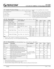
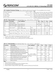
1.5V/1.8V/2.5V, 180MHz, 1:4 Networking Clock Buffer
Storage Temperature ...........................................................–65°C to +150°C
V
DD
Voltage ..........................................................................–0.5V to +2.6V
Output Voltage ............................................................... –0.5V to V
DD
+0.5V
Input Voltage .......................................................................................... 3.6V
1.5V Absolute Maximum Ratings (Above which the useful life may be impaired. For user guidelines only, not tested.)
Note:
Stresses greater than those listed under MAXIMUM
RAT INGS may cause permanent damage to the
device. This is a stress rating only and functional op er a tion
of the device at these or any other con di tions above those
indicated in the operational sec tions of this spec i fi ca tion is
not implied. Ex po sure to absolute maximum rating con di-
tions for extended periods may affect re li abil i ty.
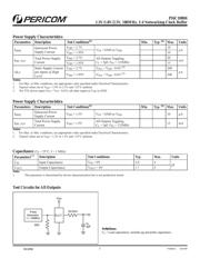
1.5V DC Characteristics (Over Operating Range: V
DD
= 1.5V ± 0.075V, T
A
= -40° to 85°C)
Parameters Description
Test Conditions
(1)
Min.
Typ.
(2)
Max. Units
V
DD
Supply Voltage 1.4 1.5 1.6
VV
IH
Input HIGH Voltage Logic HIGH level 1.17 3.6
V
IL
Input LOW Voltage Logic LOW level -0.3 0.63
I
I
Input Current
V
DD
= Max, V
IN
=
V
DD
or GND
I pins 15 μA
V
OH
Output High Voltage
V
DD
= Min., V
IN
=
V
IH
or V
IL
I
OH
= -2mA 1.05
V
I
OH
= -8mA 0.75
V
OL
Output LOW Voltage
V
DD
= Min., V
IN
-
V
IH
or V
IL
I
OL
= 1mA 0.4
I
OL
= 2mA 0.35
I
OL
= 8mA 0.35
Notes:
1. For Max. or Min. conditions, use appropriate operating range values.
2. Typical values are at V
DD
= 1.5V, +25°C ambient and maximum loading.
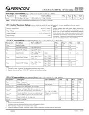
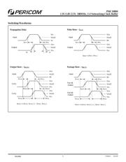
1.5V AC Characteristics (Over Operating Range: V
DD
= 1.5V ± 0.075V, T
A
= -40° to 85°C)
Parameters De scrip tion
Test Conditions
(1)
Min. Typ Max. Units
F
IN
Input Frequency 0 200 MHz
t
R
/t
F
CLKn Rise/Fall Time 20% to 80% 1.5
ns
t
PLH,
t
PHL
(2)
Propagation Delay BUF_IN to CLKn
C
L
= 5pF, 125 MHz
Outputs are measured
@ V
DD
/2
1.0 1.5 3.0
t
SK(O)
(3)
Output to Output Skew between any two out-
puts of the same device @ same transition
100
ps
t
SK(T)
(3)
Part to Part Skew between two identical out-
puts of different parts on the same board
(4)
300
t
dc_in
Duty Cycle In @ 1ns edge rate 45 55
%
t
dc_out
Duty Cycle Out 40 60
Notes:
1. See test circuit and waveforms.
2. Minimum limits are guaranteed but not tested on Propagation Delays.
3. Skew measured at worse cast temperature (max. temp).
4. Identical conditions: loading, transitions, supply voltage, temperature, package type and speed grade.
Switching Characteristics (V
DD
= 2.5V ± 0.2V or 1.8V ± 0.15V, T
A
= 105°C)
Parameters Description Test Conditions Min. Typ. Max. Units
t
R
,t
F
CLKn Rise/Fall Time 20% to 80%, C
L
= 15pF, 125MHz 0.8 1.4 ns
Note: 1. All other AC and DC characteristics are identical to the 1.8V and 2.5V sections.
09-0056
器件 Datasheet 文档搜索
AiEMA 数据库涵盖高达 72,405,303 个元件的数据手册,每天更新 5,000 多个 PDF 文件
