Datasheet 搜索 > 微控制器 > Microchip(微芯) > PIC12C672-04E/P 数据手册 > PIC12C672-04E/P 数据手册 39/130 页
 器件3D模型
¥ 27.448
PIC12C672-04E/P 数据手册 - Microchip(微芯)
制造商:
Microchip(微芯)
分类:
微控制器
封装:
PDIP-8
描述:
PIC12 系列 128 B RAM 2 K x 14位 EPROM 8位 CMOS 微控制器 - PDIP-8
Pictures:
3D模型
符号图
焊盘图
引脚图
产品图
页面导航:
引脚图在P1P9Hot
原理图在P8P26P27P28P29P30P34P39P42P47P57P65
标记信息在P115
封装信息在P115P116P117P118
功能描述在P3
技术参数、封装参数在P49P58P67P100
应用领域在P3
电气规格在P49P58
导航目录
PIC12C672-04E/P数据手册
Page:
of 130 Go
若手册格式错乱,请下载阅览PDF原文件
1997-2013 Microchip Technology Inc. DS30561C-page 39
PIC12C67X
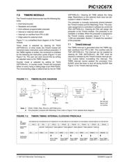
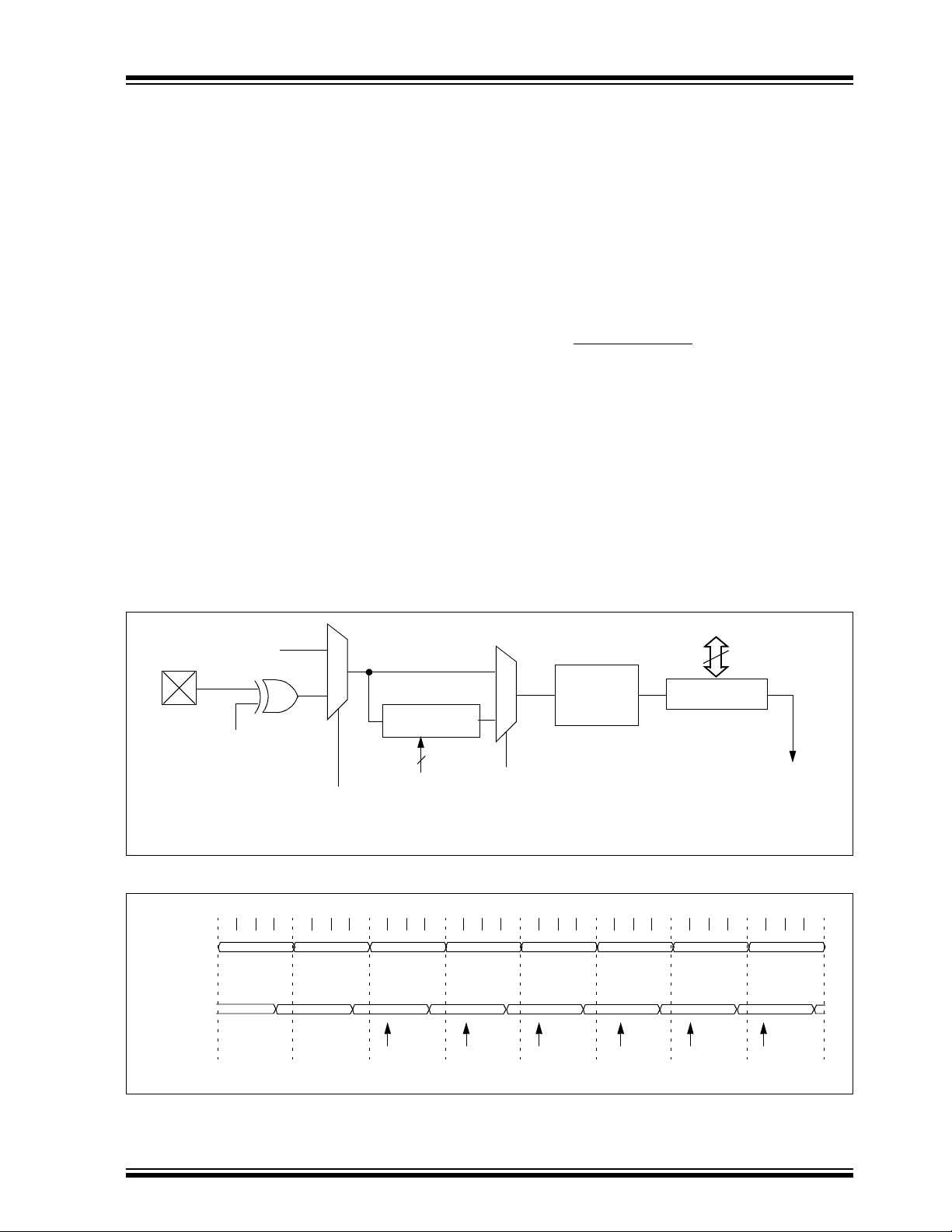
7.0 TIMER0 MODULE
The Timer0 module timer/counter has the following fea-
tures:
• 8-bit timer/counter
• Readable and writable
• 8-bit software programmable prescaler
• Internal or external clock select
• Interrupt on overflow from FFh to 00h
• Edge select for external clock
Figure 7-1 is a simplified block diagram of the Timer0
module.
Timer mode is selected by clearing bit T0CS
(OPTION<5>). In timer mode, the Timer0 module will
increment every instruction cycle (without prescaler). If
the TMR0 register is written, the increment is inhibited
for the following two instruction cycles (Figure 7-2 and
Figure 7-3). The user can work around this by writing
an adjusted value to the TMR0 register.
Counter mode is selected by setting bit T0CS
(OPTION<5>). In counter mode, Timer0 will increment
either on every rising or falling edge of pin RA4/T0CKI.
The incrementing edge is determined by the bit T0SE
(OPTION<4>). Clearing bit T0SE selects the rising
edge. Restrictions on the external clock input are dis-
cussed in detail in Section 7.2.
The prescaler is mutually exclusively shared between
the Timer0 module and the Watchdog Timer. The pres-
caler assignment is controlled in software by control bit
PSA (OPTION<3>). Clearing bit PSA will assign the
prescaler to the Timer0 module. The prescaler is not
readable or writable. When the prescaler is assigned to
the Timer0 module, prescale values of 1:2, 1:4, ...,
1:256 are selectable. Section 7.3 details the operation
of the prescaler.
7.1 Timer0 Interrupt
The TMR0 interrupt is generated when the TMR0 reg-
ister overflows from FFh to 00h. This overflow sets bit
T0IF (INTCON<2>). The interrupt can be masked by
clearing bit T0IE (INTCON<5>). Bit T0IF must be
cleared in software by the Timer0 module interrupt ser-
vice routine before re-enabling this interrupt. The
TMR0 interrupt cannot awaken the processor from
SLEEP, since the timer is shut off during SLEEP. See
Figure 7-4 for Timer0 interrupt timing.
FIGURE 7-1: TIMER0 BLOCK DIAGRAM
FIGURE 7-2: TIMER0 TIMING: INTERNAL CLOCK/NO PRESCALE
Note 1: TOCS, TOSE, PSA, PS<2:0> (OPTION<5:0>).
2: The prescaler is shared with Watchdog Timer (refer to Figure 7-6 for detailed block diagram).
GP2/TOCKI/
TOSE
0
1
1
0
AN2/INT
TOCS
FOSC/4
Programmable
Prescaler
Sync with
Internal
clocks
TMR0
(2 TCY delay)
Data Bus
8
PSA
PS<2:0>
Set interrupt
flag bit T0IF
on overflow
3
PC-1
Q1 Q2 Q3 Q4
Q1 Q2 Q3 Q4 Q1 Q2 Q3 Q4 Q1 Q2 Q3 Q4 Q1 Q2 Q3 Q4 Q1 Q2 Q3 Q4 Q1 Q2 Q3 Q4 Q1 Q2 Q3 Q4
PC
(Program
Counter)
Instruction
Fetch
TMR0
PC PC+1 PC+2 PC+3 PC+4 PC+5 PC+6
T0
T0+1 T0+2 NT0 NT0 NT0 NT0+1 NT0+2 T0
MOVWF TMR0
MOVF TMR0,WMOVF TMR0,WMOVF TMR0,WMOVF TMR0,WMOVF TMR0,W
Write TMR0
executed
Read TMR0
reads NT0
Read TMR0
reads NT0
Read TMR0
reads NT0
Read TMR0
reads NT0 + 1
Read TMR0
reads NT0 + 2
Instruction
Executed
器件 Datasheet 文档搜索
AiEMA 数据库涵盖高达 72,405,303 个元件的数据手册,每天更新 5,000 多个 PDF 文件
