Datasheet 搜索 > 微控制器 > Microchip(微芯) > PIC16C74A-20E/P 数据手册 > PIC16C74A-20E/P 数据手册 43/289 页
 器件3D模型
¥ 112.052
PIC16C74A-20E/P 数据手册 - Microchip(微芯)
制造商:
Microchip(微芯)
分类:
微控制器
封装:
PDIP-40
描述:
PIC16 系列 192 B RAM 4 K x 14位 EPROM 8位 CMOS 微控制器 - PDIP-40
Pictures:
3D模型
符号图
焊盘图
引脚图
产品图
页面导航:
引脚图在P2P3P13P14P15P16P72P73Hot
原理图在P10P11P12P43P45P46P48P50P51P54P59P62
标记信息在P260P261P262
封装信息在P251
功能描述在P5
应用领域在P166
导航目录
PIC16C74A-20E/P数据手册
Page:
of 289 Go
若手册格式错乱,请下载阅览PDF原文件
1997 Microchip Technology Inc. DS30390E-page 43
PIC16C7X
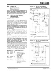
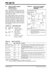
5.0 I/O PORTS
Some pins for these I/O ports are multiplexed with an
alternate function for the peripheral features on the
device. In general, when a peripheral is enabled, that
pin may not be used as a general purpose I/O pin.
5.1 PORTA and TRISA Registers
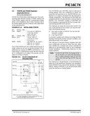
PORTA is a 6-bit latch.
The RA4/T0CKI pin is a Schmitt Trigger input and an
open drain output. All other RA port pins have TTL input
levels and full CMOS output drivers. All pins have data
direction bits (TRIS registers) which can configure
these pins as output or input.
Setting a TRISA register bit puts the corresponding out-
put driver in a hi-impedance mode. Clearing a bit in the
TRISA register puts the contents of the output latch on
the selected pin(s).
Reading the PORTA register reads the status of the
pins whereas writing to it will write to the port latch. All
write operations are read-modify-write operations.
Therefore a write to a port implies that the port pins are
read, this value is modified, and then written to the port
data latch.
Pin RA4 is multiplexed with the Timer0 module clock
input to become the RA4/T0CKI pin.
Other PORTA pins are multiplexed with analog inputs
and analog V
REF input. The operation of each pin is
selected by clearing/setting the control bits in the
ADCON1 register (A/D Control Register1).
The TRISA register controls the direction of the RA
pins, even when they are being used as analog inputs.
The user must ensure the bits in the TRISA register are
maintained set when using them as analog inputs.
EXAMPLE 5-1: INITIALIZING PORTA
BCF STATUS, RP0 ;
BCF STATUS, RP1 ; PIC16C76/77 only
CLRF PORTA ; Initialize PORTA by
; clearing output
; data latches
BSF STATUS, RP0 ; Select Bank 1
MOVLW 0xCF ; Value used to
; initialize data
; direction
MOVWF TRISA ; Set RA<3:0> as inputs
; RA<5:4> as outputs
; TRISA<7:6> are always
; read as '0'.
Applicable Devices
72
73 73A 74 74A 76 77
Applicable Devices
72
73 73A 74 74A 76 77
Note: On a Power-on Reset, these pins are con-
figured as analog inputs and read as '0'.
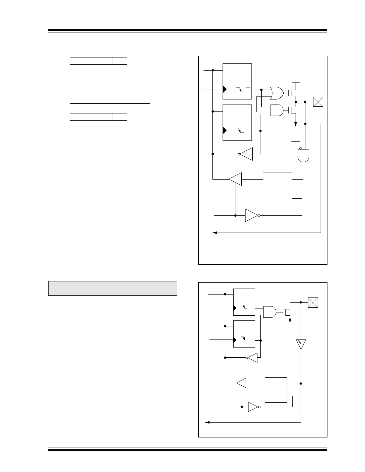
FIGURE 5-1: BLOCK DIAGRAM OF
RA3:RA0 AND RA5 PINS
FIGURE 5-2: BLOCK DIAGRAM OF RA4/
T0CKI PIN
Data
bus
QD
Q
CK
QD
Q
CK
QD
EN
P
N
WR
Port
WR
TRIS
Data Latch
TRIS Latch
RD TRIS
RD PORT
V
SS
VDD
I/O pin
(1)
Note 1: I/O pins have protection diodes to VDD and
VSS.
Analog
input
mode
TTL
input
buffer
To A/D Converter
Data
bus
WR
PORT
WR
TRIS
RD PORT
Data Latch
TRIS Latch
RD TRIS
Schmitt
Trigger
input
buffer
N
V
SS
I/O pin
(1)
TMR0 clock input
Note 1: I/O pin has protection diodes to V
SS only.
QD
Q
CK
QD
Q
CK
EN
QD
EN
器件 Datasheet 文档搜索
AiEMA 数据库涵盖高达 72,405,303 个元件的数据手册,每天更新 5,000 多个 PDF 文件
