Datasheet 搜索 > Microchip(微芯) > PIC16F84T-04B 数据手册 > PIC16F84T-04B 数据手册 27/124 页


¥ 0
PIC16F84T-04B 数据手册 - Microchip(微芯)
制造商:
Microchip(微芯)
Pictures:
3D模型
符号图
焊盘图
引脚图
产品图
页面导航:

导航目录
PIC16F84T-04B数据手册
Page:
of 124 Go
若手册格式错乱,请下载阅览PDF原文件
PIC16F8X
1998 Microchip Technology Inc. DS30430C-page 27
6.0 TIMER0 MODULE AND TMR0
REGISTER
The Timer0 module timer/counter has the following
features:
• 8-bit timer/counter
• Readable and writable
• 8-bit software programmable prescaler
• Internal or external clock select
• Interrupt on overflow from FFh to 00h
• Edge select for external clock
Timer mode is selected by clearing the T0CS bit
(OPTION_REG<5>). In timer mode, the Timer0 mod-
ule (Figure 6-1) will increment every instruction cycle
(without prescaler). If the TMR0 register is written, the
increment is inhibited for the following two cycles
(Figure 6-2 and Figure 6-3). The user can work around
this by writing an adjusted value to the TMR0 register.
Counter mode is selected by setting the T0CS bit
(OPTION_REG<5>). In this mode TMR0 will increment
either on every rising or falling edge of pin RA4/T0CKI.
The incrementing edge is determined by the T0 source
edge select bit, T0SE (OPTION_REG<4>). Clearing bit
T0SE selects the rising edge. Restrictions on the exter-
nal clock input are discussed in detail in Section 6.2.
The prescaler is shared between the Timer0 Module
and the Watchdog Timer. The prescaler assignment is
controlled, in software, by control bit PSA
(OPTION_REG<3>). Clearing bit PSA will assign the
prescaler to the Timer0 Module. The prescaler is not
readable or writable. When the prescaler (Section 6.3)
is assigned to the Timer0 Module, the prescale value
(1:2, 1:4, ..., 1:256) is software selectable.
6.1 TMR0 Interrupt
The TMR0 interrupt is generated when the TMR0
register overflows from FFh to 00h. This overflow sets
the T0IF bit (INTCON<2>). The interrupt can be
masked by clearing enable bit T0IE (INTCON<5>). The
T0IF bit must be cleared in software by the Timer0
Module interrupt service routine before re-enabling this
interrupt. The TMR0 interrupt (Figure 6-4) cannot wake
the processor from SLEEP since the timer is shut off
during SLEEP.
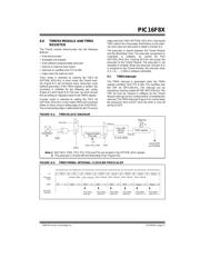
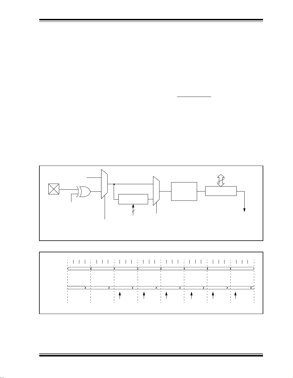
FIGURE 6-1: TMR0 BLOCK DIAGRAM
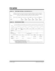
FIGURE 6-2: TMR0 TIMING: INTERNAL CLOCK/NO PRESCALER
Note 1: Bits T0CS, T0SE, PS2, PS1, PS0 and PSA are located in the OPTION_REG register.
2: The prescaler is shared with the Watchdog Timer (Figure 6-6)
RA4/T0CKI
T0SE
0
1
1
0
pin
T0CS
FOSC/4
Programmable
Prescaler
Sync with
Internal
clocks
TMR0 register
PSout
(2 cycle delay)
PSout
Data bus
8
Set bit T0IF
on Overflow
PSA
PS2, PS1, PS0
3
PC-1
Q1 Q2 Q3 Q4
Q1 Q2 Q3 Q4 Q1 Q2 Q3 Q4 Q1 Q2 Q3 Q4 Q1 Q2 Q3 Q4 Q1 Q2 Q3 Q4 Q1 Q2 Q3 Q4 Q1 Q2 Q3 Q4
PC
Instruction
Fetch
TMR0
PC PC+1 PC+2
PC+3
PC+4
PC+5 PC+6
T0
T0+1 T0+2 NT0 NT0 NT0
NT0+1 NT0+2
T0
MOVWF TMR0
MOVF TMR0,W
MOVF TMR0,W MOVF TMR0,W MOVF TMR0,W MOVF TMR0,W
Write TMR0
executed
Read TMR0
reads NT0
Read TMR0
reads NT0
Read TMR0
reads NT0
Read TMR0
reads NT0 + 1
Read TMR0
reads NT0 + 2
Instruction
Executed
器件 Datasheet 文档搜索
AiEMA 数据库涵盖高达 72,405,303 个元件的数据手册,每天更新 5,000 多个 PDF 文件
