Datasheet 搜索 > 8位微控制器 > Microchip(微芯) > PIC16LF628A-I/SS 数据手册 > PIC16LF628A-I/SS 数据手册 33/180 页
 器件3D模型
¥ 27.605
PIC16LF628A-I/SS 数据手册 - Microchip(微芯)
制造商:
Microchip(微芯)
分类:
8位微控制器
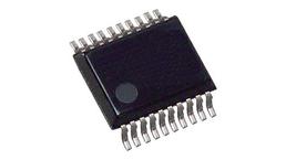
封装:
SSOP-20
描述:
MICROCHIP PIC16LF628A-I/SS 微控制器, 8位, 闪存, PIC16LF6xx, 20 MHz, 3.5 KB, 224 Byte, 20 引脚, SSOP
Pictures:
3D模型
符号图
焊盘图
引脚图
产品图
页面导航:
引脚图在P4P13P14P58P59Hot
原理图在P12P33P34P35P36P38P39P40P41P42P43P44
标记信息在P163
封装信息在P163P179
功能描述在P7
技术参数、封装参数在P51P52P100P103P111P142P144
应用领域在P101
电气规格在P51P52P100P103
导航目录
PIC16LF628A-I/SS数据手册
Page:
of 180 Go
若手册格式错乱,请下载阅览PDF原文件
© 2009 Microchip Technology Inc. DS40044G-page 33
PIC16F627A/628A/648A
5.0 I/O PORTS
The PIC16F627A/628A/648A have two ports, PORTA
and PORTB. Some pins for these I/O ports are
multiplexed with alternate functions for the peripheral
features on the device. In general, when a peripheral is
enabled, that pin may not be used as a general
purpose I/O pin.
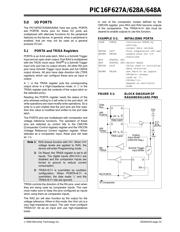
5.1 PORTA and TRISA Registers
PORTA is an 8-bit wide latch. RA4 is a Schmitt Trigger
input and an open drain output. Port RA4 is multiplexed
with the T0CKI clock input. RA5
(1)
is a Schmitt Trigger
input only and has no output drivers. All other RA port
pins have Schmitt Trigger input levels and full CMOS
output drivers. All pins have data direction bits (TRIS
registers) which can configure these pins as input or
output.
A ‘1’ in the TRISA register puts the corresponding
output driver in a High-impedance mode. A ‘0’ in the
TRISA register puts the contents of the output latch on
the selected pin(s).
Reading the PORTA register reads the status of the
pins whereas writing to it will write to the port latch. All
write operations are read-modify-write operations. So a
write to a port implies that the port pins are first read,
then this value is modified and written to the port data
latch.
The PORTA pins are multiplexed with comparator and
voltage reference functions. The operation of these
pins are selected by control bits in the CMCON
(Comparator Control register) register and the VRCON
(Voltage Reference Control register) register. When
selected as a comparator input, these pins will read
as ‘0’s.
TRISA controls the direction of the RA pins, even when
they are being used as comparator inputs. The user
must make sure to keep the pins configured as inputs
when using them as comparator inputs.
The RA2 pin will also function as the output for the
voltage reference. When in this mode, the V
REF pin is a
very high-impedance output. The user must configure
TRISA<2> bit as an input and use high-impedance
loads.
In one of the comparator modes defined by the
CMCON register, pins RA3 and RA4 become outputs
of the comparators. The TRISA<4:3> bits must be
cleared to enable outputs to use this function.
EXAMPLE 5-1: INITIALIZING PORTA
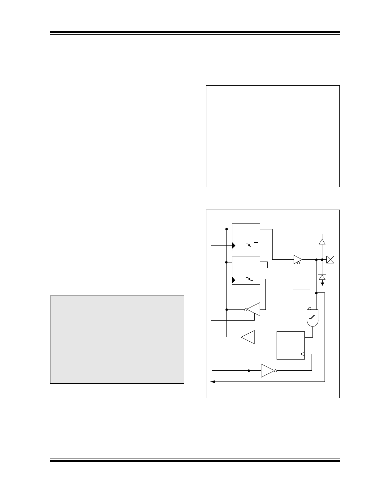
FIGURE 5-1: BLOCK DIAGRAM OF
RA0/AN0:RA1/AN1 PINS
Note 1: RA5 shares function with VPP. When VPP
voltage levels are applied to RA5, the
device will enter Programming mode.
2: On Reset, the TRISA register is set to all
inputs. The digital inputs (RA<3:0>) are
disabled and the comparator inputs are
forced to ground to reduce current
consumption.
3: TRISA<6:7> is overridden by oscillator
configuration. When PORTA<6:7> is
overridden, the data reads ‘0’ and the
TRISA<6:7> bits are ignored.
CLRF PORTA ;Initialize PORTA by
;setting
;output data latches
MOVLW 0x07 ;Turn comparators off and
MOVWF CMCON ;enable pins for I/O
;functions
BCF STATUS, RP1
BSF STATUS, RP0 ;Select Bank1
MOVLW 0x1F ;Value used to initialize
;data direction
MOVWF TRISA ;Set RA<4:0> as inputs
;TRISA<5> always
;read as ‘1’.
;TRISA<7:6>
;depend on oscillator
;mode
Data
Bus
QD
Q
CK
WR
PORTA
WR
TRISA
Data Latch
TRIS Latch
RD
RD PORTA
Analog
I/O Pin
QD
Q
CK
Input Mode
DQ
EN
To Comparator
Schmitt Trigger
Input Buffer
VDD
VSS
TRISA
(CMCON Reg.)
器件 Datasheet 文档搜索
AiEMA 数据库涵盖高达 72,405,303 个元件的数据手册,每天更新 5,000 多个 PDF 文件
