Datasheet 搜索 > 8位微控制器 > Microchip(微芯) > PIC18F25K20T-I/ML 数据手册 > PIC18F25K20T-I/ML 数据手册 135/440 页
 器件3D模型
¥ 21.541
PIC18F25K20T-I/ML 数据手册 - Microchip(微芯)
制造商:
Microchip(微芯)
分类:
8位微控制器
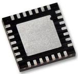
封装:
QFN-28
描述:
MICROCHIP PIC18F25K20T-I/ML 微控制器, 8位, 闪存, AEC-Q100, PIC18FxxKxx, 64 MHz, 32 KB, 1.5 KB, 28 引脚, QFN
Pictures:
3D模型
符号图
焊盘图
引脚图
产品图
页面导航:
引脚图在P3P116P135P136P138P163Hot
典型应用电路图在P184
原理图在P12P14P15P26P34P39P48P131P137P138P140P146
封装尺寸在P413
标记信息在P410P411P412
封装信息在P410P414P415P416P418P422P423P426P427P428P432P433
技术参数、封装参数在P11P12P36P93P260P264P266P269P272P273P361P362
应用领域在P30P166P173P280
电气规格在P11P12P36P93P260P264P266P269P272P273
导航目录
PIC18F25K20T-I/ML数据手册
Page:
of 440 Go
若手册格式错乱,请下载阅览PDF原文件
2010-2015 Microchip Technology Inc. DS40001303H-page 135
PIC18F2XK20/4XK20
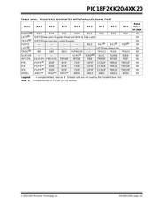
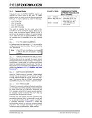
11.1 CCP Module Configuration
Each Capture/Compare/PWM module is associated
with a control register (generically, CCPxCON) and a
data register (CCPRx). The data register, in turn, is
comprised of two 8-bit registers: CCPRxL (low byte)
and CCPRxH (high byte). All registers are both
readable and writable.
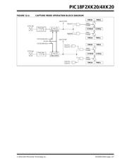
11.1.1 CCP MODULES AND TIMER
RESOURCES
The CCP modules utilize Timers 1, 2 or 3, depending
on the mode selected. Timer1 and Timer3 are available
to modules in Capture or Compare modes, while
Timer2 is available for modules in PWM mode.
TABLE 11-1: CCP MODE – TIMER
RESOURCE
The assignment of a particular timer to a module is
determined by the Timer-to-CCP enable bits in the
T3CON register (Register 15-1). Both modules can be
active at the same time and can share the same timer
resource if they are configured to operate in the same
mode (Capture/Compare or PWM). The interactions
between the two modules are summarized in Figure 11-1
and Figure 11-2. In Asynchronous Counter mode, the
capture operation will not work reliably.
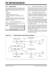
11.1.2 CCP2 PIN ASSIGNMENT
The pin assignment for CCP2 (Capture input, Compare
and PWM output) can change, based on device config-
uration. The CCP2MX Configuration bit determines the
pin with which CCP2 is multiplexed. By default, it is
assigned to RC1 (CCP2MX = 1). If the Configuration bit
is cleared, CCP2 is multiplexed with RB3.
Changing the pin assignment of CCP2 does not
automatically change any requirements for configuring
the port pin. Users must always verify that the
appropriate TRIS register is configured correctly for
CCP2 operation, regardless of where it is located.
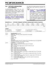
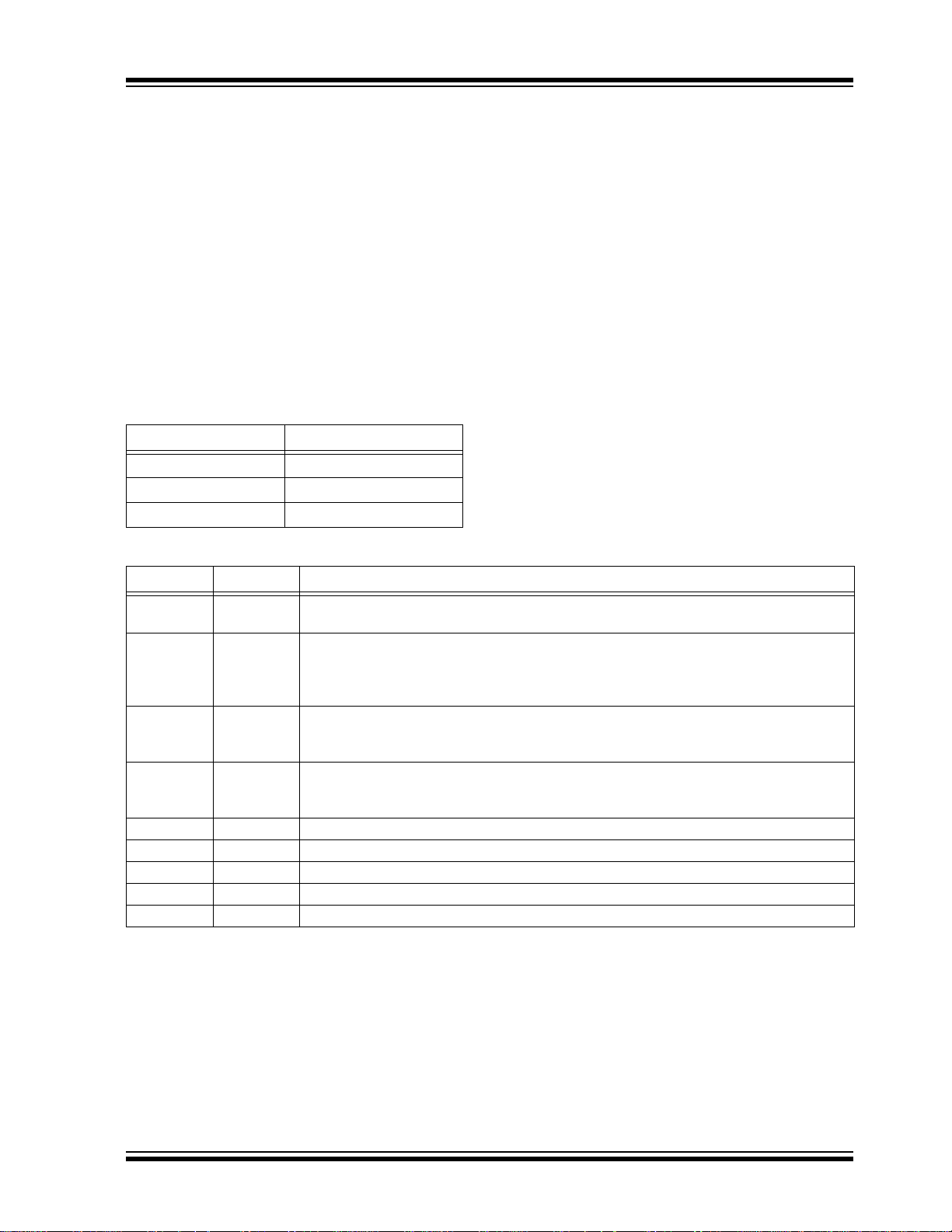
TABLE 11-2: INTERACTIONS BETWEEN CCP1 AND CCP2 FOR TIMER RESOURCES
CCP/ECCP Mode Timer Resource
Capture Timer1 or Timer3
Compare Timer1 or Timer3
PWM Timer2
CCP1 Mode CCP2 Mode Interaction
Capture Capture Each module can use TMR1 or TMR3 as the time base. The time base can be different
for each CCP.
Capture Compare CCP2 can be configured for the Special Event Trigger to reset TMR1 or TMR3
(depending upon which time base is used). Automatic A/D conversions on trigger event
can also be done. Operation of CCP1 could be affected if it is using the same timer as a
time base.
Compare Capture CCP1 can be configured for the Special Event Trigger to reset TMR1 or TMR3
(depending upon which time base is used). Operation of CCP2 could be affected if it is
using the same timer as a time base.
Compare Compare Either module can be configured for the Special Event Trigger to reset the time base.
Automatic A/D conversions on CCP2 trigger event can be done. Conflicts may occur if
both modules are using the same time base.
Capture PWM None
Compare PWM None
PWM
(1)
Capture None
PWM
(1)
Compare None
PWM
(1)
PWM Both PWMs will have the same frequency and update rate (TMR2 interrupt).
Note 1: Includes standard and enhanced PWM operation.
器件 Datasheet 文档搜索
AiEMA 数据库涵盖高达 72,405,303 个元件的数据手册,每天更新 5,000 多个 PDF 文件
