Datasheet 搜索 > Microchip(微芯) > PIC18LF4620T-E/PT 数据手册 > PIC18LF4620T-E/PT 数据手册 146/412 页

 器件3D模型
¥ 0
PIC18LF4620T-E/PT 数据手册 - Microchip(微芯)
制造商:
Microchip(微芯)
封装:
TQFP
Pictures:
3D模型
符号图
焊盘图
引脚图
产品图
页面导航:
引脚图在P4P5P142P143P144P150Hot
典型应用电路图在P167
原理图在P10P12P13P27P43P108P126P130P136P138P143P144
封装尺寸在P387
标记信息在P385P386
封装信息在P385
技术参数、封装参数在P338P340P343P344P345
应用领域在P154P248
电气规格在P9P10P75P236P237P241P242P245
导航目录
PIC18LF4620T-E/PT数据手册
Page:
of 412 Go
若手册格式错乱,请下载阅览PDF原文件
PIC18F2525/2620/4525/4620
DS39626E-page 144 © 2008 Microchip Technology Inc.
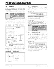
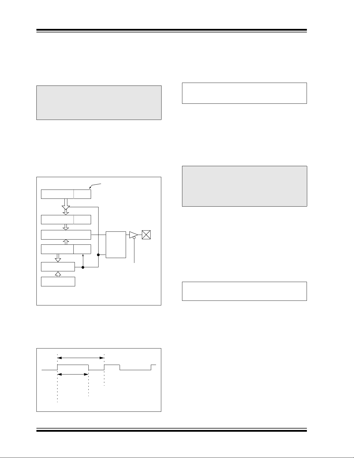
15.4 PWM Mode
In Pulse-Width Modulation (PWM) mode, the CCPx pin
produces up to a 10-bit resolution PWM output. Since
the CCP2 pin is multiplexed with a PORTB or PORTC
data latch, the appropriate TRIS bit must be cleared to
make the CCP2 pin an output.
Figure 15-3 shows a simplified block diagram of the
CCP module in PWM mode.
For a step-by-step procedure on how to set up the CCP
module for PWM operation, see Section 15.4.4
“Setup for PWM Operation”.
FIGURE 15-3: SIMPLIFIED PWM BLOCK
DIAGRAM
A PWM output (Figure 15-4) has a time base (period)
and a time that the output stays high (duty cycle).
The frequency of the PWM is the inverse of the
period (1/period).
FIGURE 15-4: PWM OUTPUT
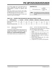
15.4.1 PWM PERIOD
The PWM period is specified by writing to the PR2
register. The PWM period can be calculated using the
following formula:
EQUATION 15-1:
PWM frequency is defined as 1/[PWM period].
When TMR2 is equal to PR2, the following three events
occur on the next increment cycle:
•TMR2 is cleared
• The CCPx pin is set (exception: if PWM duty
cycle = 0%, the CCPx pin will not be set)
• The PWM duty cycle is latched from CCPRxL into
CCPRxH
15.4.2 PWM DUTY CYCLE
The PWM duty cycle is specified by writing to the
CCPRxL register and to the CCPxCON<5:4> bits. Up
to 10-bit resolution is available. The CCPRxL contains
the eight MSbs and the CCPxCON<5:4> contains the
two LSbs. This 10-bit value is represented by
CCPRxL:CCPxCON<5:4>. The following equation is
used to calculate the PWM duty cycle in time:
EQUATION 15-2:
CCPRxL and CCPxCON<5:4> can be written to at any
time, but the duty cycle value is not latched into
CCPR2H until after a match between PR2 and TMR2
occurs (i.e., the period is complete). In PWM mode,
CCPRxH is a read-only register.
Note: Clearing the CCP2CON register will force
the RB3 or RC1 output latch (depending on
device configuration) to the default low
level. This is not the PORTB or PORTC I/O
data latch.
CCPRxL
CCPRxH (Slave)
Comparator
TMR2
Comparator
PR2
(Note 1)
R
Q
S
Duty Cycle Registers
CCPxCON<5:4>
Clear Timer,
CCPx pin and
latch D.C.
Note 1: The 8-bit TMR2 value is concatenated with the 2-bit
internal Q clock, or 2 bits of the prescaler, to create the
10-bit time base.
CCPx Output
Corresponding
TRIS bit
Period
Duty Cycle
TMR2 = PR2
TMR2 = Duty Cycle
TMR2 = PR2
Note: The Timer2 postscalers (see Section 13.0
“Timer2 Module”) are not used in the
determination of the PWM frequency. The
postscaler could be used to have a servo
update rate at a different frequency than
the PWM output.
PWM Period = [(PR2) + 1] • 4 • TOSC •
(TMR2 Prescale Value)
PWM Duty Cycle = (CCPRXL:CCPXCON<5:4>) •
T
OSC • (TMR2 Prescale Value)
器件 Datasheet 文档搜索
AiEMA 数据库涵盖高达 72,405,303 个元件的数据手册,每天更新 5,000 多个 PDF 文件
