Datasheet 搜索 > Microchip(微芯) > PIC24FJ64GA705-I/M4 数据手册 > PIC24FJ64GA705-I/M4 数据手册 167/412 页
 器件3D模型
¥ 3.857
PIC24FJ64GA705-I/M4 数据手册 - Microchip(微芯)
制造商:
Microchip(微芯)
封装:
UQFN-48
描述:
16位微控制器 - MCU 16-bit, 16 MIPS, 64KB Flash, 16KB RAM
Pictures:
3D模型
符号图
焊盘图
引脚图
产品图
页面导航:
引脚图在P3P4P5P6P7P8P9P10P20P21P22P23Hot
典型应用电路图在P318P319
原理图在P19P36P63P79P125P159P162P163P167P174P176P183
封装尺寸在P377
标记信息在P375P376
封装信息在P358P375P380P381P382P383P384P385P387P389P390P391
功能描述在P3P4P6P8P10P167P173P239P251
技术参数、封装参数在P114P221P359P364P365P366P367P368P370P373
应用领域在P80P81
电气规格在P31P114P126P224P225P328P341
导航目录
PIC24FJ64GA705-I/M4数据手册
Page:
of 412 Go
若手册格式错乱,请下载阅览PDF原文件
2016 Microchip Technology Inc. DS30010118B-page 167
PIC24FJ256GA705 FAMILY
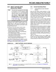
14.0 INPUT CAPTURE WITH
DEDICATED TIMERS
Devices in the PIC24FJ256GA705 family contain three
independent input capture modules. Each of the
modules offers a wide range of configuration and
operating options for capturing external pulse events
and generating interrupts.
Key features of the input capture module include:
• Hardware-Configurable for 32-Bit Operation in
All modes by Cascading Two Adjacent modules
• Synchronous and Trigger modes of Output
Compare Operation with up to 31 User-Selectable
Sync/Trigger Sources Available
• A 4-Level FIFO Buffer for Capturing and Holding
Timer Values for Several Events
• Configurable Interrupt Generation
• Up to 6 Clock Sources Available for Each module,
Driving a Separate Internal 16-Bit Counter
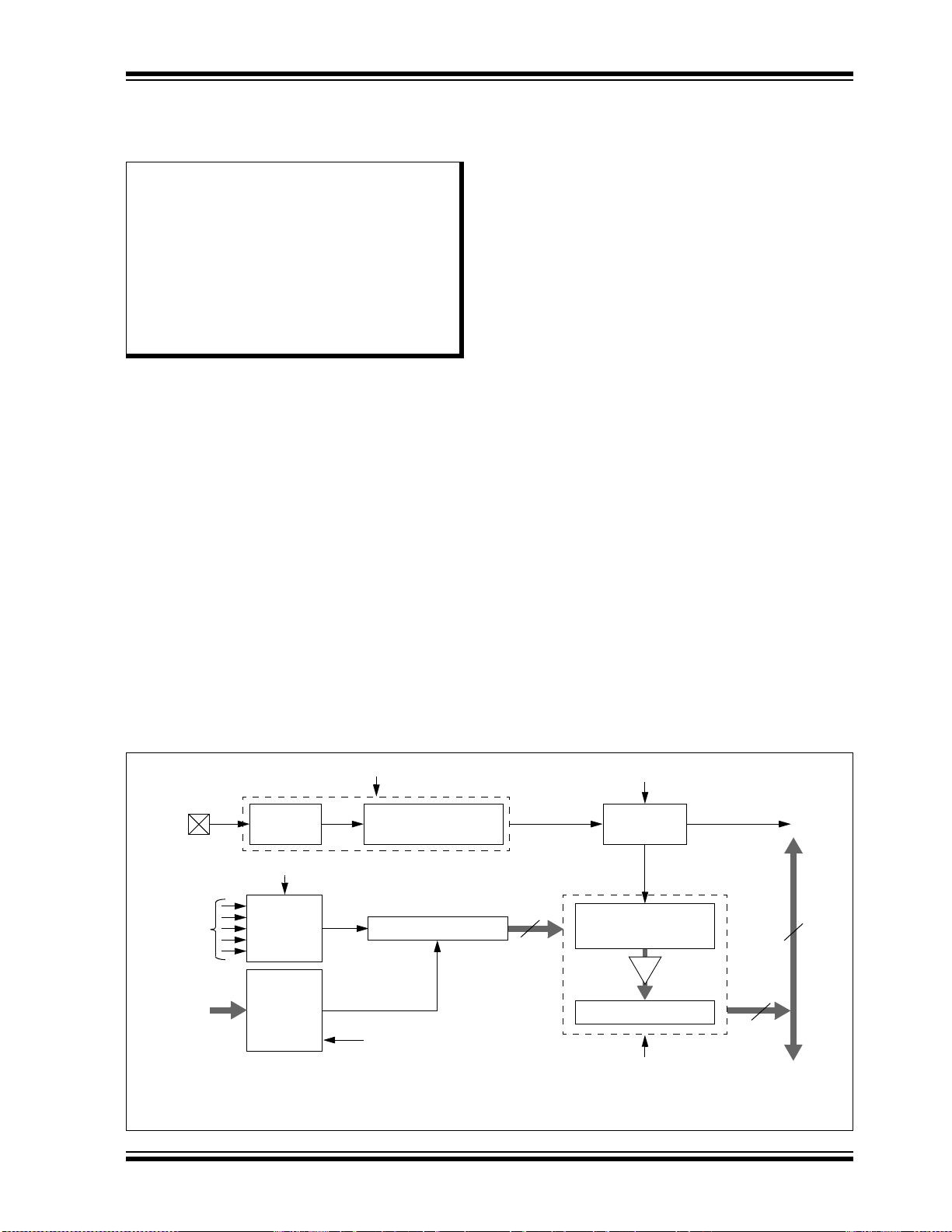
The module is controlled through two registers: ICxCON1
(Register 14-1) and ICxCON2 (Register 14-2). A general
block diagram of the module is shown in Figure 14-1.
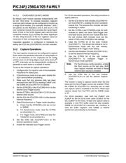
14.1 General Operating Modes
14.1.1 SYNCHRONOUS AND TRIGGER
MODES
When the input capture module operates in a Free-
Running mode, the internal 16-bit counter, ICxTMR,
counts up continuously, wrapping around from FFFFh
to 0000h on each overflow. Its period is synchronized
to the selected external clock source. When a capture
event occurs, the current 16-bit value of the internal
counter is written to the FIFO buffer.
In Synchronous mode, the module begins capturing
events on the ICx pin as soon as its selected clock
source is enabled. Whenever an event occurs on the
selected Sync source, the internal counter is reset. In
Trigger mode, the module waits for a Sync event from
another internal module to occur before allowing the
internal counter to run.
Standard, free-running operation is selected by setting
the SYNCSEL<4:0> bits (ICxCON2<4:0>) to ‘00000’
and clearing the ICTRIG bit (ICxCON2<7>). Synchro-
nous and Trigger modes are selected any time the
SYNCSELx bits are set to any value except ‘00000’.
The ICTRIG bit selects either Synchronous or Trigger
mode; setting the bit selects Trigger mode operation. In
both modes, the SYNCSELx bits determine the Sync/
Trigger source.
When the SYNCSELx bits are set to ‘00000’ and
ICTRIG is set, the module operates in Software Trigger
mode. In this case, capture operations are started by
manually setting the TRIGSTAT bit (ICxCON2<6>).
FIGURE 14-1: INPUT CAPTURE x BLOCK DIAGRAM
Note: This data sheet summarizes the features
of this group of PIC24F devices. It is
not intended to be a comprehensive
reference source. For more information,
refer to the “dsPIC33/PIC24 Family Refer-
ence Manual”, ”Input Capture with
Dedicated Timer” (DS70000352), which
is available from the Microchip web site
(www.microchip.com). The information
in this data sheet supersedes the
information in the FRM.
Note 1: The ICx input must be assigned to an available RPn/RPIn pin before use. See Section 11.5 “Peripheral Pin
Select (PPS)” for more information.
ICxBUF
4-Level FIFO Buffer
ICx Pin
(1)
ICM<2:0>
Set ICxIF
Edge Detect Logic
ICI<1:0>
ICOV, ICBNE
System Bus
Prescaler
Counter
1:1/4/16
and
Clock Synchronizer
Clock
Select
ICx Clock
Sources
Sync and
ICTSEL<2:0>
SYNCSEL<4:0>
Trigger
16
16
16
Increment
Reset
Sync and
Trigger
Logic
Trigger Sources
ICxTMR
Interrupt
Logic
Event and
器件 Datasheet 文档搜索
AiEMA 数据库涵盖高达 72,405,303 个元件的数据手册,每天更新 5,000 多个 PDF 文件
