Datasheet 搜索 > Microchip(微芯) > PIC24FJ64GA705-I/M4 数据手册 > PIC24FJ64GA705-I/M4 数据手册 183/412 页
 器件3D模型
¥ 3.857
PIC24FJ64GA705-I/M4 数据手册 - Microchip(微芯)
制造商:
Microchip(微芯)
封装:
UQFN-48
描述:
16位微控制器 - MCU 16-bit, 16 MIPS, 64KB Flash, 16KB RAM
Pictures:
3D模型
符号图
焊盘图
引脚图
产品图
页面导航:
引脚图在P3P4P5P6P7P8P9P10P20P21P22P23Hot
典型应用电路图在P318P319
原理图在P19P36P63P79P125P159P162P163P167P174P176P183
封装尺寸在P377
标记信息在P375P376
封装信息在P358P375P380P381P382P383P384P385P387P389P390P391
功能描述在P3P4P6P8P10P167P173P239P251
技术参数、封装参数在P114P221P359P364P365P366P367P368P370P373
应用领域在P80P81
电气规格在P31P114P126P224P225P328P341

导航目录
PIC24FJ64GA705-I/M4数据手册
Page:
of 412 Go
若手册格式错乱,请下载阅览PDF原文件
2016 Microchip Technology Inc. DS30010118B-page 183
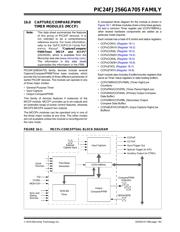
PIC24FJ256GA705 FAMILY
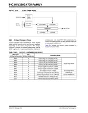
16.0 CAPTURE/COMPARE/PWM/
TIMER MODULES (MCCP)
PIC24FJ256GA705 family devices include several
Capture/Compare/PWM/Timer base modules, which
provide the functionality of three different peripherals of
earlier PIC24F devices. The module can operate in one
of three major modes:
• General Purpose Timer
• Input Capture
• Output Compare/PWM
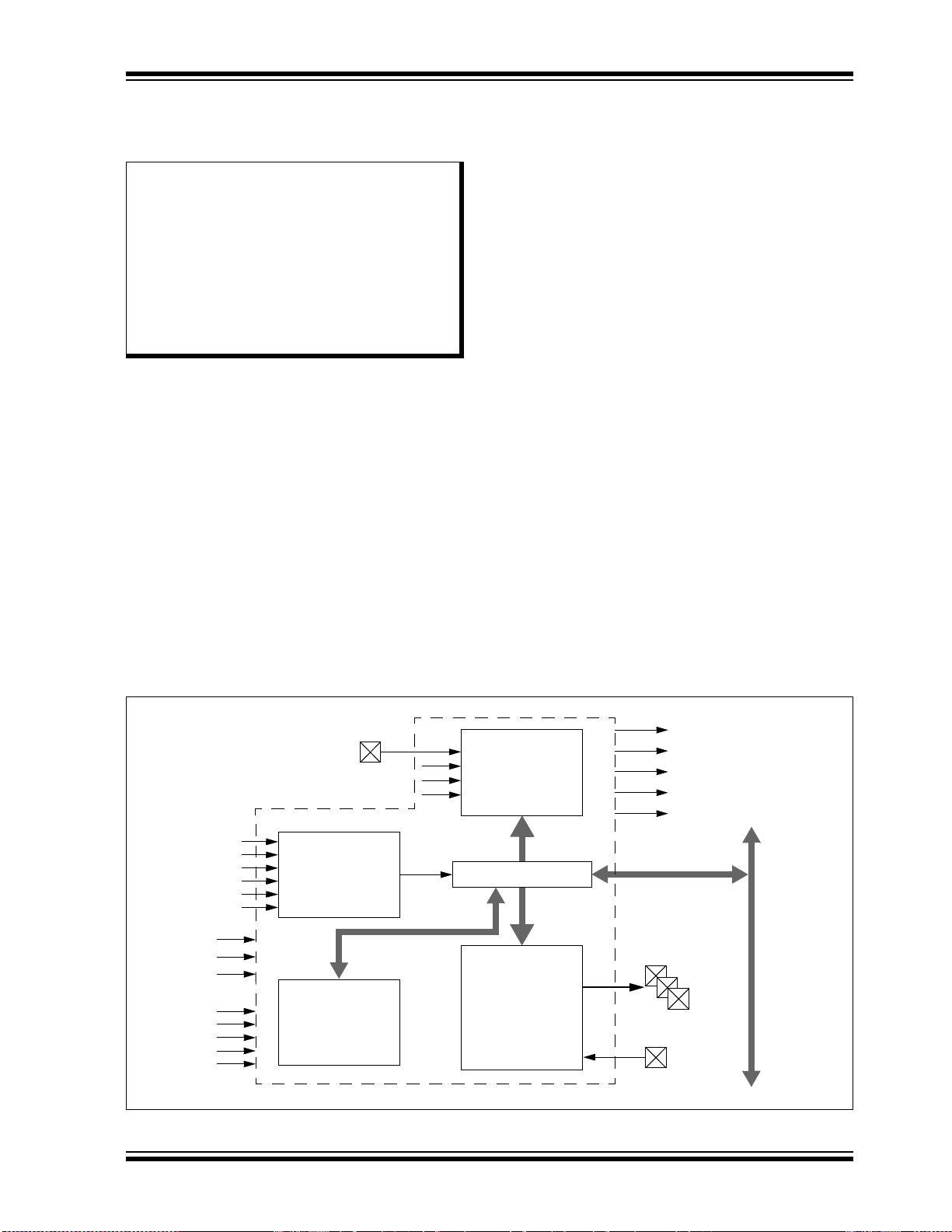
This family of devices features 4 instances of the
MCCP module. MCCP1 provides up to six outputs and
an extended range of power control features, whereas
MCCP2-MCCP4 support two outputs.
The MCCPx modules can be operated only in one of
the three major modes at any time. The other modes
are not available unless the module is reconfigured for
the new mode.
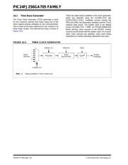
A conceptual block diagram for the module is shown in
Figure 16-1. All three modules share a time base genera-
tor and a common Timer register pair (CCPxTMRH/L);
other shared hardware components are added as a
particular mode requires.
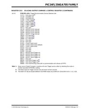
Each module has a total of 8 control and status registers:
• CCPxCON1L (Register 16-1)
• CCPxCON1H (Register 16-2)
• CCPxCON2L (Register 16-3)
• CCPxCON2H (Register 16-4)
• CCPxCON3L (Register 16-5)
• CCPxCON3H (Register 16-6)
• CCPxSTATL (Register 16-7)
• CCPxSTATH (Register 16-8)
Each module also includes 8 buffer/counter registers that
serve as Timer Value registers or data holding buffers:
• CCPxTMRH/CCPxTMRL (Timer High/Low
Counters)
• CCPxPRH/CCPxPRL (Timer Period High/Low)
• CCPxRAH/CCPxRAL (Primary Output Compare
Data Buffer)
• CCPxRBH/CCPxRBL (Secondary Output
Compare Data Buffer)
• CCPxBUFH/CCPxBUFL (Input Capture High/Low
Buffers)
FIGURE 16-1: MCCPx CONCEPTUAL BLOCK DIAGRAM
Note: This data sheet summarizes the features
of this group of PIC24F devices. It is
not intended to be a comprehensive
reference source. For more information,
refer to the “dsPIC33/PIC24 Family Ref-
erence Manual”, “Capture/Compare/
PWM/Timer (MCCP and SCCP)”
(DS33035), which is available from the
Microchip web site (www.microchip.com).
The information in this data sheet
supersedes the information in the FRM.
Clock
Sources
Input Capture
Output
Compare/PWM
T32
CCSEL
MOD<3:0>
Sync and
Gating
Sources
16/32-Bit
Auxiliary Output (to CTMU)
CCPxIF
CCTxIF
External
Compare/PWM
Output(s)
OEFA/OEFB
Timer
Sync/Trigger Out
Special Trigger (to A/D)
Capture Input
Time Base
Generator
CCPxTMRH/L
器件 Datasheet 文档搜索
AiEMA 数据库涵盖高达 72,405,303 个元件的数据手册,每天更新 5,000 多个 PDF 文件
