Datasheet 搜索 > NXP(恩智浦) > PN5180A0ET/C1,118 数据手册 > PN5180A0ET/C1,118 数据手册 63/126 页
 器件3D模型
¥ 34.671
PN5180A0ET/C1,118 数据手册 - NXP(恩智浦)
制造商:
NXP(恩智浦)
封装:
TFBGA-64
Pictures:
3D模型
符号图
焊盘图
引脚图
产品图
页面导航:
引脚图在P7P8P40Hot
原理图在P7P63
封装尺寸在P101P102
型号编码规则在P4
标记信息在P5P6
封装信息在P97P98P99P100
焊接温度在P103P104
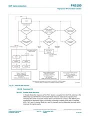
功能描述在P1P2P9P63
技术参数、封装参数在P123
应用领域在P3P123
导航目录
PN5180A0ET/C1,118数据手册
Page:
of 126 Go
若手册格式错乱,请下载阅览PDF原文件
PN5180 All information provided in this document is subject to legal disclaimers. © NXP Semiconductors N.V. 2015. All rights reserved.
Preliminary data sheet
COMPANY PUBLIC
Rev. 2.2 — 17 December 2015
240922 63 of 126
NXP Semiconductors
PN5180
High-power NFC frontend solution
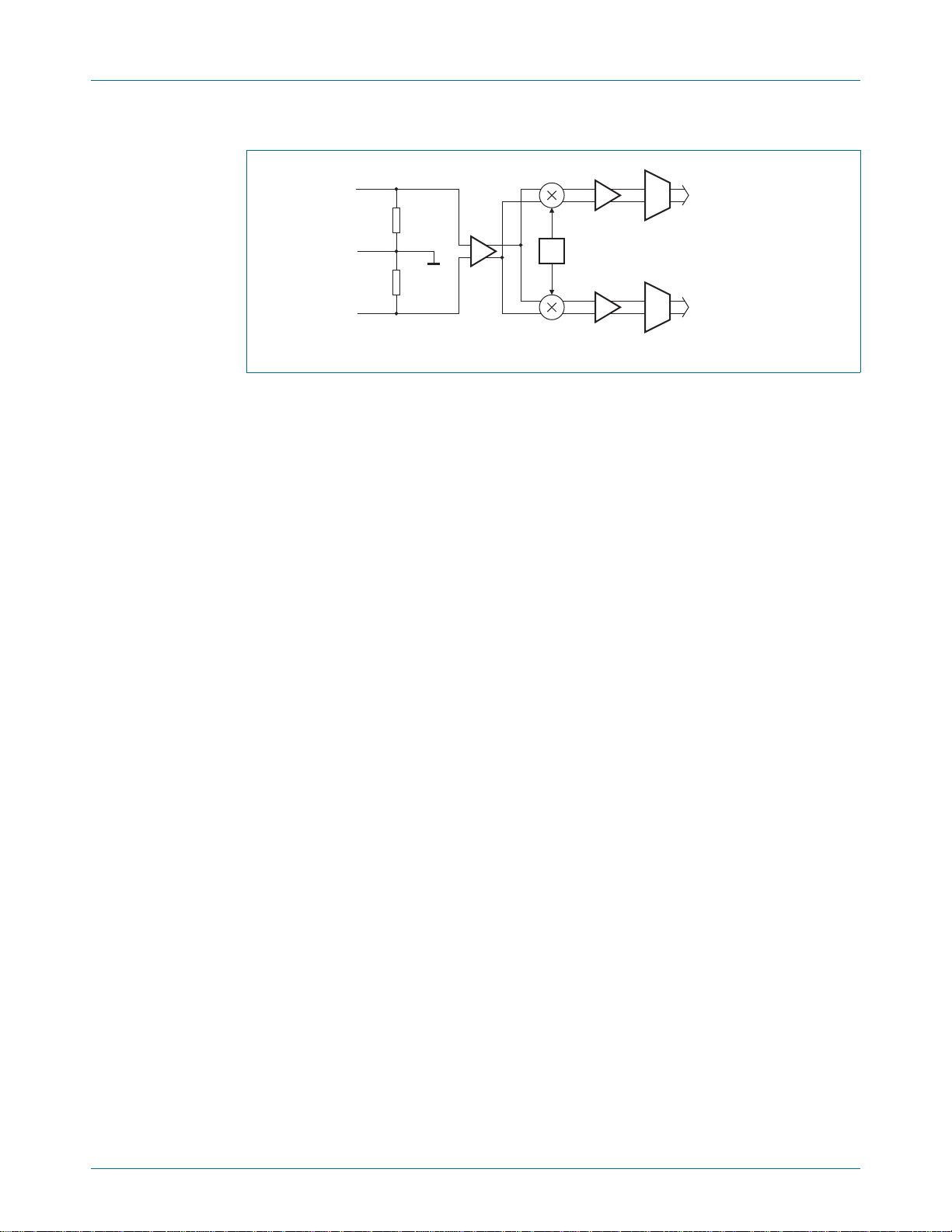
10.8.8.2 VMID
The input voltage for PIN Vmid is generated by a resistive divider between AVDD and
GND. The resistive divider is connected to the VMID pin, an external blocking capacitor
shall be placed there.
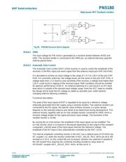
10.8.8.3 Automatic Gain Control
The Automatic Gain Control (AGC) of the receiver is used to control the amplitude of the
received 13.56 MHz input sine-wave signal from the antenna (input pins RXP and RXN).
It is desirable to achieve an input voltage in the range of 1.5 V to 1.65 V at the pins RXP,
RXN. For symmetric antennas, the voltage levels are the same on the pins RXP, RXN. A
voltage lower than 1.5 V lead to a low sensitivity of the receiver, a voltage level higher than
1.65 V could result in clipping of the received signal. Both conditions should be avoided
for optimum performance of the IC. An antenna detuning of a card result in an RX input
level which is outside of the desired input voltage range. Here the AGC helps to simplify
the design and to keep the RX voltage as stable as possible even under dynamic
changing antenna detuning conditions.
Functional description:
The peak of the input signal at RXP is regulated to be equal to a reference voltage
(internally generated from the supply using a resistive divider). Two external resistors are
connected to the RX inputs, the specific value of these resistors in a given design
depends on the selected antenna and needs to be determined during development. This
external resistor, together with an on-chip variable resistor connected to VMID, forms a
resistive voltage divider for the signal processor input voltage. The resolution of the
variable resistor is 10 bits.
By varying the on-chip resistor, the amplitude of the input signal can be modified. The
on-chip resistor value is increased or decreased depending on the output of the sampled
comparator, until the peak of the input signal matches the reference voltage. The
amplitude of the RX input is thus automatically controlled by the AGC circuit.
The internal amplitude controlling resistor in the AGC has a default value of 10 kOhm typ
DC coupled. (i.e. when the resistor control bits in AGC_VALUE_REG <9:0> are all 0, the
resistance is 10 k). As the control bits are increased, resistors are switched in parallel to
the 10k resistor thus lowering the combined resulting resistance value down to
20 OhmDC coupled (AGC_VALUE_REG <9:0>, all bits set to 1).
Fig 28. PN5180 Receiver Block diagram
aaa-008644
RXP
V
MID
AGC
BBA
BBA
MIX
CLK
I-CLK
Q-CLK
RXN
DATA
DATA
器件 Datasheet 文档搜索
AiEMA 数据库涵盖高达 72,405,303 个元件的数据手册,每天更新 5,000 多个 PDF 文件
