Datasheet 搜索 > 电压基准芯片 > ADI(亚德诺) > REF198GSZ 数据手册 > REF198GSZ 数据手册 1/28 页
 器件3D模型
¥ 42.603
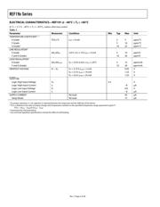
REF198GSZ 数据手册 - ADI(亚德诺)
制造商:
ADI(亚德诺)
分类:
电压基准芯片
封装:
SOIC-8
描述:
ANALOG DEVICES REF198GSZ 电压基准, 精准微功率, 系列 - 固定, REF198系列, 4.096V, NSOIC-8
Pictures:
3D模型
符号图
焊盘图
引脚图
产品图
页面导航:
引脚图在P1Hot
原理图在P19
封装尺寸在P25
型号编码规则在P26
功能描述在P1
技术参数、封装参数在P1P3P15
应用领域在P1P19P22
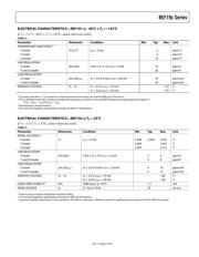
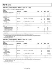
电气规格在P3P4P5P6P7P8P9P10P11P12P13P14
导航目录
REF198GSZ数据手册
Page:
of 28 Go
若手册格式错乱,请下载阅览PDF原文件
Precision Micropower, Low Dropout
Voltage References
REF19x Series
Rev. I
Information furnished by Analog Devices is believed to be accurate and reliable. However, no
responsibility is assumed by Analog Devices for its use, nor for any infringements of patents or other
rights of third parties that may result from its use. Specifications subject to change without notice. No
license is granted by implication or otherwise under any patent or patent rights of Analog Devices.
Trademarks and registered trademarks are the property of their respective owners.
One Technology Way, P.O. Box 9106, Norwood, MA 02062-9106, U.S.A.
Tel: 781.329.4700 www.analog.com
Fax: 781.461.3113 ©2006 Analog Devices, Inc. All rights reserved.
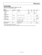
FEATURES
Initial accuracy: ±2 mV maximum
Temperature coefficient: 5 ppm/°C maximum
Low supply current: 45 μA maximum
Sleep mode: 15 μA maximum
Low dropout voltage
Load regulation: 4 ppm/mA
Line regulation: 4 ppm/V
High output current: 30 mA
Short-circuit protection
APPLICATIONS
Portable instruments
ADCs and DACs
Smart sensors
Solar-powered applications
Loop current-powered instruments
GENERAL DESCRIPTION
The REF19x series precision band gap voltage references use a
patented temperature drift curvature correction circuit and
laser trimming of highly stable, thin-film resistors to achieve a
very low temperature coefficient and high initial accuracy.
The REF19x series is made up of micropower, low dropout
voltage (LDV) devices, providing stable output voltage from
supplies as low as 100 mV above the output voltage and
consuming less than 45 μA of supply current. In sleep mode,
which is enabled by applying a low TTL or CMOS level to the
SLEEP
pin, the output is turned off, and supply current is
further reduced to less than 15 μA.
The REF19x series references are specified over the extended
industrial temperature range (−40°C to +85°C), with typical
performance specifications over −40°C to +125°C for
applications such as automotive.
All electrical grades are available in an 8-lead SOIC_N package;
the PDIP and TSSOP packages are available only in the lowest
electrical grade. Products are also available in die form.
TEST PINS
Test Pin 1 and Test Pin 5 are reserved for in-package Zener zap.
To achieve the highest level of accuracy at the output, the Zener
zapping technique is used to trim the output voltage. Since each
unit may require a different amount of adjustment, the resistance
value at the test pins varies widely from pin to pin and from
part to part. The user should leave Pin 1 and Pin 5
unconnected.
REF19x
SERIES
TOP VIEW
(Not to Scale)
TP
1
V
S
2
SLEEP
3
GND
4
NC
NC
OUTPUT
TP
8
7
6
5
NOTES
1. NC = NO CONNECT.
2. TP PINS ARE FACTORY TEST
POINTS, NO USER CONNECTION.
0
0371-001
Figure 1. 8-Lead SOIC_N and TSSOP Pin Configuration
(S Suffix and RU Suffix)
REF19x
SERIES
TOP VIEW
(Not to Scale)
TP
1
V
S
2
S
LEEP
3
GND
4
NC
NC
OUTPUT
TP
8
7
6
5
NOTES
1. NC = NO CONNECT.
2. TP PINS ARE FACTORY TEST
POINTS, NO USER CONNECTION.
00371-002
Figure 2. 8-Lead PDIP Pin Configuration
(P Suffix)
Table 1. Nominal Output Voltage
Part Number Nominal Output Voltage (V)
REF191 2.048
REF192 2.50
REF193 3.00
REF194 4.50
REF195 5.00
REF196 3.30
REF198 4.096
器件 Datasheet 文档搜索
AiEMA 数据库涵盖高达 72,405,303 个元件的数据手册,每天更新 5,000 多个 PDF 文件
