Datasheet 搜索 > 电压基准芯片 > TI(德州仪器) > REF3212AIDBVTG4 数据手册 > REF3212AIDBVTG4 数据手册 4/19 页

¥ 34.125
REF3212AIDBVTG4 数据手册 - TI(德州仪器)
制造商:
TI(德州仪器)
分类:
电压基准芯片
封装:
SOT-23-6
描述:
TEXAS INSTRUMENTS REF3212AIDBVTG4 电压基准, 微功率, 低压降, 系列 - 固定, REF3212系列, 1.25V, SOT-23-6
Pictures:
3D模型
符号图
焊盘图
引脚图
产品图
页面导航:
引脚图在P2Hot
典型应用电路图在P11
原理图在P8
封装尺寸在P2P14P15
标记信息在P2P14P15
封装信息在P2P14P15P16
功能描述在P2P8
技术参数、封装参数在P2
应用领域在P1P4P16
电气规格在P3P4P8
导航目录
REF3212AIDBVTG4数据手册
Page:
of 19 Go
若手册格式错乱,请下载阅览PDF原文件

REF3212, REF3220
REF3225, REF3230
REF3233, REF3240
SBVS058C –JUNE 2005– REVISED AUGUST 2011
www.ti.com
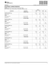
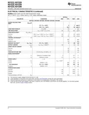
ELECTRICAL CHARACTERISTICS (continued)
Boldface limits apply over the listed temperature range.
At T
A
= +25°C, I
LOAD
= 0mA, and V
IN
= 5V, unless otherwise noted.
REF32xx
PARAMETER CONDITIONS MIN TYP MAX UNIT
REF3212 / REF3220 / REF3225 / REF3230 / REF3233 / REF3240
OUTPUT VOLTAGE TEMP
dV
OUT
/dT
DRIFT
0°C ≤ T
A
≤ +125°C 4 7 ppm/°C
–40°C ≤ T
A
≤ +125°C 10.5 20 ppm/°C
LONG-TERM STABILITY 0 to 1000h 55 ppm
LINE REGULATION V
OUT
+ 0.05
(1)
≤ V
IN
≤ 5.5V –65 15 +65 ppm/V
LOAD REGULATION
(2)
dV
OUT
/dI
LOAD
Sourcing 0mA < I
LOAD
< 10mA, V
IN
= V
OUT
+ 250mV
(1)
–40 3 40 µV/mA
Sinking –10mA < I
LOAD
< 0mA, V
IN
= V
OUT
+ 100mV
(1)
–60 20 60 µV/mA
THERMAL HYSTERESIS
(3)
dT
First cycle 100 ppm
Additional cycles 25 ppm
DROPOUT VOLTAGE
(1)
V
IN
– V
OUT
0°C ≤ T
A
≤ +125°C 5 50 mV
OUTPUT CURRENT I
LOAD
V
IN
= V
OUT
+ 250mV
(1)
–10 10 mA
SHORT-CIRCUIT CURRENT I
SC
Sourcing 50 mA
Sinking 40 mA
TURN-ON SETTLING TIME To 0.1% at V
IN
= 5V with C
L
= 0 60 µs
ENABLE/SHUTDOWN
(4)
V
L
Reference in Shutdown mode 0 0.7 V
V
H
Reference is active 1.5 V
IN
V
POWER SUPPLY I
L
= 0
Voltage V
IN
V
OUT
+ 0.05
(1)
5.5 V
Current I
Q
ENABLE > 1.5V 100 120 µA
.. Over temperature 0°C ≤ T
A
≤ +125°C 115 135 µA
Shutdown I
S
ENABLE < 0.7V 0.1 1 µA
TEMPERATURE RANGE
Specified –40 +125 °C
Operating –55 +135 °C
Storage –65 +150 °C
Thermal resistance, SOT23-6 θ
JA
200 °C/W
(1) The minimum supply voltage for the REF3212 is 1.8V.
(2) Load regulation is using force and sense lines; see the Load Regulation section for more information.
(3) Thermal hysteresis procedure is explained in more detail in the Applications Information TBD section.
(4) If the rise time of the input voltage is less than or equal to 2ms, the ENABLE and IN pins can be tied together. For rise times greater
than 2ms, see the Supply Voltage section.
4 Copyright © 2005–2011, Texas Instruments Incorporated
器件 Datasheet 文档搜索
AiEMA 数据库涵盖高达 72,405,303 个元件的数据手册,每天更新 5,000 多个 PDF 文件
