Datasheet 搜索 > 电压基准芯片 > TI(德州仪器) > REF3320AIDCKR 数据手册 > REF3320AIDCKR 数据手册 5/34 页
 器件3D模型
¥ 5.255
REF3320AIDCKR 数据手册 - TI(德州仪器)
制造商:
TI(德州仪器)
分类:
电压基准芯片
封装:
SC-70-3
描述:
3.9レA, SC70-3 ,为30ppm / ΣC漂移参考电压 3.9レA, SC70-3, 30ppm/∑C Drift VOLTAGE REFERENCE
Pictures:
3D模型
符号图
焊盘图
引脚图
产品图
页面导航:
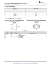
引脚图在P4Hot
典型应用电路图在P13P14P15
原理图在P11
封装尺寸在P22P23P24P26P27P28P31
焊盘布局在P32
标记信息在P22P23P24P25
封装信息在P21P22P23P24P25P26P27P28
技术参数、封装参数在P5
应用领域在P1P13P14P15
电气规格在P6P7P12P15
导航目录
REF3320AIDCKR数据手册
Page:
of 34 Go
若手册格式错乱,请下载阅览PDF原文件
5
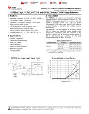
REF3312
,
REF3318
,
REF3320
,
REF3325
,
REF3330
,
REF3333
www.ti.com
SBOS392G –AUGUST 2007–REVISED DECEMBER 2016
Product Folder Links: REF3312 REF3318 REF3320 REF3325 REF3330 REF3333
Submit Documentation FeedbackCopyright © 2007–2016, Texas Instruments Incorporated
(1) Stresses beyond those listed under Absolute Maximum Ratings may cause permanent damage to the device. These are stress ratings
only, which do not imply functional operation of the device at these or any other conditions beyond those indicated under Recommended
Operating Conditions. Exposure to absolute-maximum-rated conditions for extended periods may affect device reliability.
(2) See the Power-Supply Recommendations section of this data sheet.
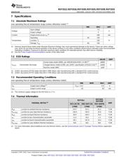
7 Specifications
7.1 Absolute Maximum Ratings
over operating free-air temperature range (unless otherwise noted).
(1)
MIN MAX UNIT
Voltage
Input voltage 7.5
V
Output voltage 5
Current Output short-circuit, I
SC
(2)
180 mA
Temperature
Operating –50 150
°CJunction, T
J
150
Storage, T
stg
–65 150
(1) JEDEC document JEP155 states that 500-V HBM allows safe manufacturing with a standard ESD control process.
(2) JEDEC document JEP157 states that 250-V CDM allows safe manufacturing with a standard ESD control process.
7.2 ESD Ratings
VALUE UNIT
V
(ESD)
Electrostatic discharge
Human body model (HBM), per ANSI/ESDA/JEDEC JS-001
(1)
±4000
VCharged device model (CDM), per JEDEC specification JESD22-C101
(2)
±1000
Machine model (MM) ±200
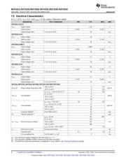
(1) The minimum supply voltage for the REF3312 is 1.7 V.
7.3 Recommended Operating Conditions
over operating free-air temperature range (unless otherwise noted).
MIN NOM MAX UNIT
V
IN
Supply input voltage
(1)
V
OUT
+ 0.2 5.5 V
I
OUT
Output current range –30 30 mA
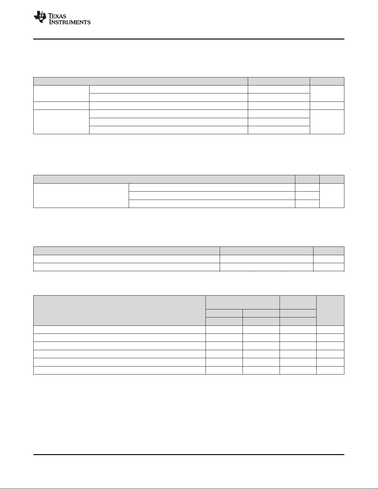
(1) For more information about traditional and new thermal metrics, see the Semiconductor and IC Package Thermal Metrics application
report.
7.4 Thermal Information
THERMAL METRIC
(1)
REF33xx
REF3325,
REF3330
UNIT
DCK (SC70) DBZ (SOT-23) RSE (UQFN)
3 PINS 3 PINS 8 PINS
R
θJA
Junction-to-ambient thermal resistance 279.7 313.1 61.2 °C/W
R
θJC(top)
Junction-to-case (top) thermal resistance 136.3 144.0 32.6 °C/W
R
θJB
Junction-to-board thermal resistance 56.9 109.3 16.0 °C/W
ψ
JT
Junction-to-top characterization parameter 11.0 18.2 1.3 °C/W
ψ
JB
Junction-to-board characterization parameter 56.1 107.9 16.0 °C/W
R
θJC(bot)
Junction-to-case (bottom) thermal resistance N/A N/A N/A °C/W
器件 Datasheet 文档搜索
AiEMA 数据库涵盖高达 72,405,303 个元件的数据手册,每天更新 5,000 多个 PDF 文件
