Datasheet 搜索 > 存储芯片 > Cypress Semiconductor(赛普拉斯) > S29AL016J70BFI022 数据手册 > S29AL016J70BFI022 数据手册 8/58 页

 器件3D模型
¥ 111.583
S29AL016J70BFI022 数据手册 - Cypress Semiconductor(赛普拉斯)
制造商:
Cypress Semiconductor(赛普拉斯)
分类:
存储芯片
封装:
FBGA-48
Pictures:
3D模型
符号图
焊盘图
引脚图
产品图
页面导航:

导航目录
S29AL016J70BFI022数据手册
Page:
of 58 Go
若手册格式错乱,请下载阅览PDF原文件
Document Number: 002-00777 Rev. *L Page 8 of 58
S29AL016J
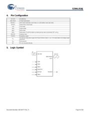
4. Pin Configuration
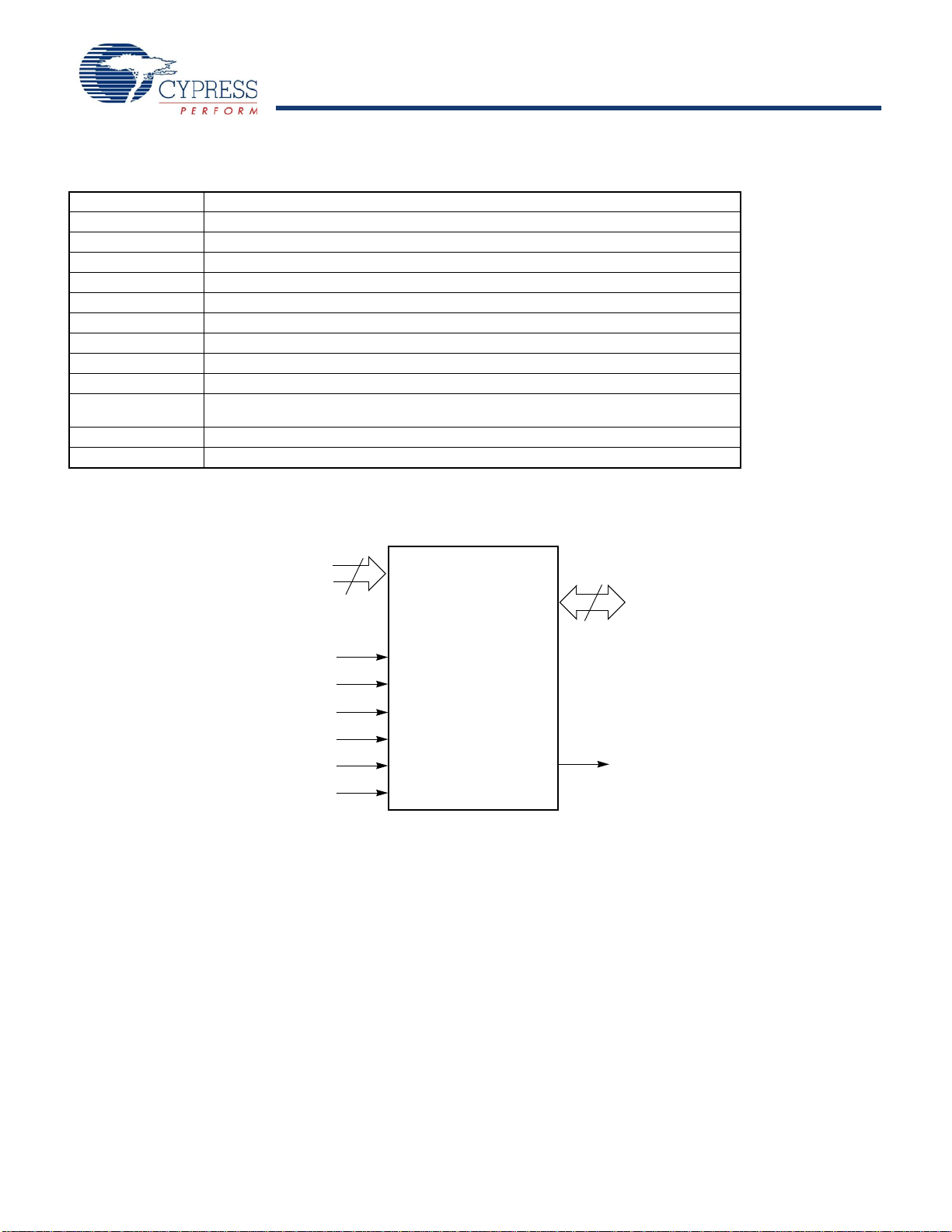
5. Logic Symbol
A0–A19 20 addresses
DQ0–DQ14 15 data inputs/outputs
DQ15/A-1 DQ15 (data input/output, word mode), A-1 (LSB address input, byte mode)
BYTE# Selects 8-bit or 16-bit mode
CE# Chip enable
OE# Output enable
WE# Write enable
WP# Write protect: The WP# contains an internal pull-up; when unconnected, WP is at V
IH
.
RESET# Hardware reset
RY/BY# Ready/Busy output
V
CC
3.0 volt-only single power supply (see Product Selector Guide on page 4 for speed options and voltage supply
tolerances)
V
SS
Device ground
NC Pin not connected internally
20
16 or 8
DQ0–DQ15
(A-1)
A0–A19
CE#
OE#
WE#
RESET#
BYTE# RY/BY#
WP#
器件 Datasheet 文档搜索
AiEMA 数据库涵盖高达 72,405,303 个元件的数据手册,每天更新 5,000 多个 PDF 文件
