Datasheet 搜索 > 存储芯片 > Cypress Semiconductor(赛普拉斯) > S29AL016J70TFI013 数据手册 > S29AL016J70TFI013 数据手册 3/58 页
 器件3D模型
¥ 40.438
S29AL016J70TFI013 数据手册 - Cypress Semiconductor(赛普拉斯)
制造商:
Cypress Semiconductor(赛普拉斯)
分类:
存储芯片
封装:
TSOP-48
描述:
闪存, 并行NOR, 16 Mbit, 2M x 8位, CFI, 并行, TSOP, 48 引脚
Pictures:
3D模型
符号图
焊盘图
引脚图
产品图
页面导航:
导航目录
S29AL016J70TFI013数据手册
Page:
of 58 Go
若手册格式错乱,请下载阅览PDF原文件

Document Number: 002-00777 Rev. *L Page 3 of 58
S29AL016J
Contents
Distinctive Characteristics .................................................. 1
General Description ............................................................. 2
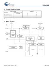
1. Product Selector Guide............................................... 4
2. Block Diagram.............................................................. 4
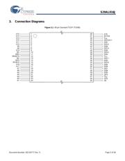
3. Connection Diagrams.................................................. 5
3.1 Special Handling Instructions......................................... 7
4. Pin Configuration......................................................... 8
5. Logic Symbol ............................................................... 8
6. Ordering Information................................................... 9
6.1 S29AL016J Standard Products...................................... 9
7. Device Bus Operations.............................................. 10
7.1 Word/Byte Configuration.............................................. 11
7.2 Requirements for Reading Array Data......................... 11
7.3 Writing Commands/Command Sequences.................. 11
7.4 Program and Erase Operation Status.......................... 12
7.5 Standby Mode.............................................................. 12
7.6 Automatic Sleep Mode................................................. 13
7.7 RESET#: Hardware Reset Pin..................................... 13
7.8 Output Disable Mode................................................... 13
7.9 Autoselect Mode.......................................................... 16
7.10 Sector Group Protection/Unprotection......................... 16
7.11 Temporary Sector Group Unprotect............................. 17
8. Secured Silicon Sector Flash Memory Region ....... 20
8.1 Factory Locked: Secured Silicon Sector Programmed
and Protected at the Factory........................................ 20
8.2 Customer Lockable: Secured Silicon Sector NOT
Programmed or Protected at the Factory..................... 20
9. Common Flash Memory Interface (CFI)................... 21
9.1 Hardware Data Protection............................................ 24
10. Command Definitions................................................ 24
10.1 Reading Array Data ..................................................... 24
10.2 Reset Command.......................................................... 25
10.3 Autoselect Command Sequence ................................. 25
10.4 Enter/Exit Secured Silicon
Sector Command
Sequence..................................................................... 25
10.5 Word/Byte Program Command Sequence................... 25
10.6 Unlock Bypass Command Sequence .......................... 26
10.7 Chip Erase Command Sequence ................................ 27
10.8 Sector Erase Command Sequence ............................. 27
10.9 Erase Suspend/Erase Resume Commands................ 27
10.10Command Definitions Table........................................ 29
11. Write Operation Status .............................................. 30
11.1 DQ7: Data# Polling...................................................... 30
11.2 RY/BY#: Ready/Busy#................................................. 31
11.3 DQ6: Toggle Bit I ......................................................... 32
11.4 DQ2: Toggle Bit II ........................................................ 32
11.5 Reading Toggle Bits DQ6/DQ2.................................... 33
11.6 DQ5: Exceeded Timing Limits ..................................... 34
11.7 DQ3: Sector Erase Timer............................................. 34
12. Absolute Maximum Ratings....................................... 35
13. Operating Ranges....................................................... 35
14. DC Characteristics...................................................... 37
14.1 CMOS Compatible........................................................ 37
15. Test Conditions........................................................... 38
16. Key to Switching Waveforms..................................... 38
17. AC Characteristics...................................................... 39
17.1 Read Operations........................................................... 39
17.2 Hardware Reset (RESET#)........................................... 40
17.3 Word/Byte Configuration (BYTE#)................................ 41
17.4 Erase/Program Operations........................................... 42
17.5 Temporary Sector Group Unprotect.............................. 46
17.6 Alternate CE# Controlled Erase/Program Operations .. 47
18. Erase and Programming Performance ..................... 48
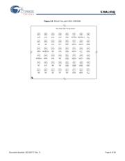
19. TSOP and BGA Pin Capacitance............................... 49
20. Physical Dimensions.................................................. 50
20.1 TS 048—48-Pin Standard TSOP.................................. 50
20.2 VBK048—48-Ball Fine-Pitch Ball Grid Array (BGA)
8.15 mm x 6.15 mm...................................................... 51
20.3 LAE064–64-Ball Fortified Ball Grid Array (BGA)
9 mm x 9 mm................................................................ 52
21. Revision History.......................................................... 53
器件 Datasheet 文档搜索
AiEMA 数据库涵盖高达 72,405,303 个元件的数据手册,每天更新 5,000 多个 PDF 文件
