Datasheet 搜索 > Flash芯片 > Cypress Semiconductor(赛普拉斯) > S29GL032N90TFI023 数据手册 > S29GL032N90TFI023 数据手册 18/81 页
 器件3D模型
¥ 20.717
S29GL032N90TFI023 数据手册 - Cypress Semiconductor(赛普拉斯)
制造商:
Cypress Semiconductor(赛普拉斯)
分类:
Flash芯片
封装:
TSOP-56
描述:
闪存, MirrorBit架构, 并行NOR, 32 Mbit, 4M x 8位, CFI, 并行, TSOP, 56 引脚
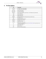
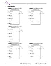
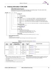
Pictures:
3D模型
符号图
焊盘图
引脚图
产品图
页面导航:
导航目录
S29GL032N90TFI023数据手册
Page:
of 81 Go
若手册格式错乱,请下载阅览PDF原文件

18 S29GL-N MirrorBit
®
Flash Family S29GL-N_01_12 October 29, 2008
Data Sheet
8.2.1 Page Mode Read
The device is capable of fast page mode read and is compatible with the page mode Mask ROM read
operation. This mode provides faster read access speed for random locations within a page. The page size of
the device is 8 words/16 bytes. The appropriate page is selected by the higher address bits A(max)–A3.
Address bits A2–A0 in word mode (A2–A-1 in byte mode) determine the specific word within a page. This is
an asynchronous operation; the microprocessor supplies the specific word location.
The random or initial page access is equal to t
ACC
or t
CE
and subsequent page read accesses (as long as the
locations specified by the microprocessor falls within that page) is equivalent to t
PACC
. When CE# is
deasserted and reasserted for a subsequent access, the access time is t
ACC
or t
CE
. Fast page mode
accesses are obtained by keeping the read-page addresses constant and changing the intra-read page
addresses.
8.3 Writing Commands/Command Sequences
To write a command or command sequence (which includes programming data to the device and erasing
sectors of memory), the system must drive WE# and CE# to V
IL
, and OE# to V
IH
.
The device features an Unlock Bypass mode to facilitate faster programming. Once the device enters the
Unlock Bypass mode, only two write cycles are required to program a word, instead of four. The Word
Program Command Sequence on page 42 contains details on programming data to the device using both
standard and Unlock Bypass command sequences.
An erase operation can erase one sector, multiple sectors, or the entire device. Tables 8.2 – 8.8 indicate the
address space that each sector occupies.
Refer to the DC Characteristics table for the active current specification for the write mode. The AC
Characteristics section contains timing specification tables and timing diagrams for write operations.
8.3.1 Write Buffer
Write Buffer Programming allows the system write to a maximum of 16 words/32 bytes in one programming
operation. This results in faster effective programming time than the standard programming algorithms.
8.3.2 Accelerated Program Operation
The device offers accelerated program operations through the ACC function. This is one of two functions
provided by the WP#/ACC or ACC pin, depending on model number. This function is primarily intended to
allow faster manufacturing throughput at the factory.
If the system asserts V
HH
on this pin, the device automatically enters the Unlock Bypass mode, temporarily
unprotects any protected sectors, and uses the higher voltage on the pin to reduce the time required for
program operations. The system would use a two-cycle program command sequence as required by the
Unlock Bypass mode. Removing V
HH
from the WP#/ACC or ACC pin, depending on model number, returns
the device to normal operation. Note that the WP#/ACC or ACC pin must not be at V
HH
for operations other
than accelerated programming, or device damage may result. WP# contains an internal pull-up; when
unconnected, WP# is at V
IH
.
8.3.3 Autoselect Functions
If the system writes the autoselect command sequence, the device enters the autoselect mode. The system
can then read autoselect codes from the internal register (which is separate from the memory array) on
DQ7-DQ0. Standard read cycle timings (t
ACC
) apply in this mode. Refer to Autoselect Mode on page 29 and
Autoselect Command Sequence on page 42 for more information.
器件 Datasheet 文档搜索
AiEMA 数据库涵盖高达 72,405,303 个元件的数据手册,每天更新 5,000 多个 PDF 文件
