Datasheet 搜索 > 存储芯片 > Spansion(飞索半导体) > S29JL064J70BHI003 数据手册 > S29JL064J70BHI003 数据手册 1/59 页

 器件3D模型
¥ 17.593
S29JL064J70BHI003 数据手册 - Spansion(飞索半导体)
制造商:
Spansion(飞索半导体)
分类:
存储芯片
封装:
VFBGA
Pictures:
3D模型
符号图
焊盘图
引脚图
产品图
页面导航:
导航目录
S29JL064J70BHI003数据手册
Page:
of 59 Go
若手册格式错乱,请下载阅览PDF原文件

Cypress Semiconductor Corporation • 198 Champion Court • San Jose, CA 95134-1709 • 408-943-2600
Document Number: 002-00856 Rev. *E Revised December 08, 2015
S29JL064J
64 Mbit (8 M x 8-Bit/4 M x 16-Bit), 3 V
Simultaneous Read/Write Flash
Distinctive Characteristics
Architectural Advantages
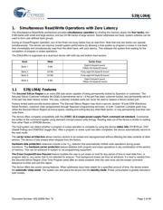
Simultaneous Read/Write operations
– Data can be continuously read from one bank while executing
erase/program functions in another bank
– Zero latency between read and write operations
Flexible bank architecture
– Read may occur in any of the three banks not being programmed
or erased
– Four banks may be grouped by customer to achieve desired bank
divisions
Boot sectors
– Top and bottom boot sectors in the same device
– Any combination of sectors can be erased
Manufactured on 0.11 µm Process Technology
Secured Silicon Region: Extra 256-byte sector
– Factory locked and identifiable: 16 bytes available for secure,
random factory Electronic Serial Number; verifiable as factory
locked through autoselect function
– Customer lockable: One-time programmable only. Once locked,
data cannot be changed
Zero power operation
– Sophisticated power management circuits reduce power
consumed during inactive periods to nearly zero
Compatible with JEDEC standards
– Pinout and software compatible with single-power-supply flash
standard
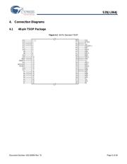
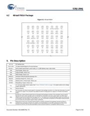
Package Options
48-ball Fine-pitch BGA
48-pin TSOP
Performance Characteristics
High performance
– Access time as fast as 55 ns
– Program time: 7 µs/word typical using accelerated programming
function
Ultra low power consumption (typical values)
– 2 mA active read current at 1 MHz
– 10 mA active read current at 5 MHz
– 200 nA in standby or automatic sleep mode
Cycling endurance: 1 million cycles per sector typical
Data retention: 20 years typical
Software Features
Supports Common Flash Memory Interface (CFI)
Erase suspend/erase resume
– Suspends erase operations to read data from, or program data to,
a sector that is not being erased, then resumes the erase
operation
Data# polling and toggle bits
– Provides a software method of detecting the status of program or
erase operations
Unlock bypass program command
– Reduces overall programming time when issuing multiple program
command sequences
Hardware Features
Ready/Busy# output (RY/BY#)
– Hardware method for detecting program or erase cycle
completion
Hardware reset pin (RESET#)
– Hardware method of resetting the internal state machine to the
read mode
WP#/ACC input pin
– Write protect (WP#) function protects sectors 0, 1, 140, and 141,
regardless of sector protect status
– Acceleration (ACC) function accelerates program timing
Sector Protection
– Hardware method to prevent any program or erase operation
within a sector
– Temporary Sector Unprotect allows changing data in protected
sectors in-system
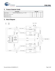
General Description
The S29JL064J is a 64 Mbit, 3.0 volt-only flash memory device, organized as 4,194,304 words of 16 bits each or 8,388,608 bytes of
8 bits each. Word mode data appears on DQ15–DQ0; byte mode data appears on DQ7–DQ0. The device is designed to be
programmed in-system with the standard 3.0 volt V
CC
supply, and can also be programmed in standard EPROM programmers. The
device is available with an access time of 55, 60, 70 ns and is offered in a 48-ball FBGA or 48-pin TSOP package. Standard control
pins—chip enable (CE#), write enable (WE#), and output enable (OE#)—control normal read and write operations, and avoid bus
contention issues. The device requires only a single 3.0 volt power supply for both read and write functions. Internally generated
and regulated voltages are provided for the program and erase operations.
器件 Datasheet 文档搜索
AiEMA 数据库涵盖高达 72,405,303 个元件的数据手册,每天更新 5,000 多个 PDF 文件
