Datasheet 搜索 > 稳压芯片 > TI(德州仪器) > SG3524N 数据手册 > SG3524N 数据手册 4/30 页
 器件3D模型
¥ 4.284
SG3524N 数据手册 - TI(德州仪器)
制造商:
TI(德州仪器)
分类:
稳压芯片
封装:
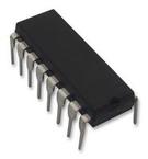
PDIP-16
描述:
TEXAS INSTRUMENTS SG3524N 调整控制器, PWM, 40V-8V电源, 450 kHz, 5.4V/100mA输出, DIP-16
Pictures:
3D模型
符号图
焊盘图
引脚图
产品图
页面导航:
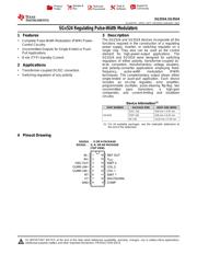
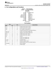
引脚图在P3Hot
典型应用电路图在P12P14P15
原理图在P9P11P14P16P17
封装尺寸在P21P23P24
标记信息在P21P22
封装信息在P20P21P22P23P24
技术参数、封装参数在P4
应用领域在P1P30
电气规格在P5P6
型号编号列表在P4
导航目录
SG3524N数据手册
Page:
of 30 Go
若手册格式错乱,请下载阅览PDF原文件
SG2524
,
SG3524
SLVS077E –APRIL 1977–REVISED JANUARY 2015
www.ti.com
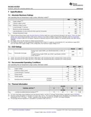
7 Specifications
7.1 Absolute Maximum Ratings
over operating free-air temperature range (unless otherwise noted)
(1)
MIN MAX UNIT
V
CC
Supply voltage
(2)(3)
40 V
I
CC
Collector output current 100 mA
I
O(ref)
Reference output current 50 mA
Current through CT terminal –5 mA
T
J
Maximum junction temperature 150 °C
Lead temperature 1,6 mm (1/16 inch) from case for 10 seconds 260 °C
T
stg
Storage temperature range –65 150 °C
(1) Stresses beyond those listed under Absolute Maximum Ratings table may cause permanent damage to the device. These are stress
ratings only, and functional operation of the device at these or any other conditions beyond those indicated under Recommended
Operating Conditions table are not implied. Exposure to absolute-maximum-rated conditions for extended periods may affect device
reliability.
(2) All voltage values are with respect to network ground terminal.
(3) The reference regulator may be bypassed for operation from a fixed 5-V supply by connecting the VCC and reference output (REF
OUT) pin both to the supply voltage. In this configuration, the maximum supply voltage is 6 V.
7.2 ESD Ratings
VALUE UNIT
Human body model (HBM), per ANSI/ESDA/JEDEC JS-001, all
1000
pins
(1)
V
(ESD)
Electrostatic discharge V
Charged device model (CDM), per JEDEC specification JESD22-
1000
C101, all pins
(2)
(1) JEDEC document JEP155 states that 500-V HBM allows safe manufacturing with a standard ESD control process.
(2) JEDEC document JEP157 states that 250-V CDM allows safe manufacturing with a standard ESD control process.
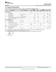
7.3 Recommended Operating Conditions
over operating free-air temperature range (unless otherwise noted)
MIN MAX UNIT
V
CC
Supply Voltage 8 40 V
Reference output current 0 50 mA
Current through CT terminal –0.03 –2 mA
R
T
Timing resistor 1.8 100 kΩ
C
T
Timing capacitor 0.001 0.1 µF
SG2524 –25 85
T
A
Operating free-air temperature °C
SG3524 0 70
7.4 Thermal Information
SGx524
THERMAL METRIC
(1)
D N NS UNIT
16 PINS
R
θJA
Junction-to-ambient thermal resistance
(2)(3)
73 67 64 °C/W
(1) For more information about traditional and new thermal metrics, see the IC Package Thermal Metrics application report, SPRA953.
(2) Maximum power dissipation is a function of T
J
(max), θJA, and T
A
. The maximum allowable power dissipation at any allowable ambient
temperature is PD = (TJ(max) – TA)/θJA. Operation at the absolute maximum TJ of 150°C can impact reliability.
(3) The package thermal impedance is calculated in accordance with JESD 51-7.
4 Submit Documentation Feedback Copyright © 1977–2015, Texas Instruments Incorporated
Product Folder Links: SG2524 SG3524
器件 Datasheet 文档搜索
AiEMA 数据库涵盖高达 72,405,303 个元件的数据手册,每天更新 5,000 多个 PDF 文件
