Datasheet 搜索 > 接口芯片 > NXP(恩智浦) > SJA1000TD 数据手册 > SJA1000TD 数据手册 5/68 页


¥ 0
SJA1000TD 数据手册 - NXP(恩智浦)
制造商:
NXP(恩智浦)
分类:
接口芯片
封装:
SOP
描述:
5V独立CAN总线控制器
Pictures:
3D模型
符号图
焊盘图
引脚图
产品图
页面导航:
导航目录
SJA1000TD数据手册
Page:
of 68 Go
若手册格式错乱,请下载阅览PDF原文件
2000 Jan 04 5
Philips Semiconductors Product specification
Stand-alone CAN controller SJA1000
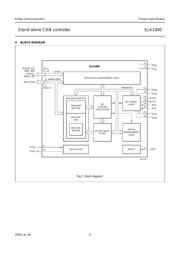
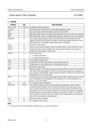
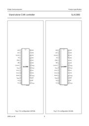
5 PINNING
Note
1. XTAL1 and XTAL2 pins should be connected to V
SS1
via 15 pF capacitors.
SYMBOL PIN DESCRIPTION
AD7 to AD0 2, 1, 28 to 23 multiplexed address/data bus
ALE/AS 3 ALE input signal (Intel mode), AS input signal (Motorola mode)
CS 4 chip select input, LOW level allows access to the SJA1000
RD/E 5 RD signal (Intel mode) or E enable signal (Motorola mode) from the microcontroller
WR 6 WR signal (Intel mode) or RD/WR signal (Motorola mode) from the microcontroller
CLKOUT 7 clock output signal produced by the SJA1000 for the microcontroller; the clock
signal is derived from the built-in oscillator via the programmable divider; the clock
off bit within the clock divider register allows this pin to disable
V
SS1
8 ground for logic circuits
XTAL1 9 input to the oscillator amplifier; external oscillator signal is input via this pin; note 1
XTAL2 10 output from the oscillator amplifier; the output must be left open-circuit when an
external oscillator signal is used; note 1
MODE 11 mode select input
1 = selects Intel mode
0 = selects Motorola mode
V
DD3
12 5 V supply for output driver
TX0 13 output from the CAN output driver 0 to the physical bus line
TX1 14 output from the CAN output driver 1 to the physical bus line
V
SS3
15 ground for output driver
INT 16 interrupt output, used to interrupt the microcontroller; INT is active LOW if any bit of
the internal interrupt register is set; INT is an open-drain output and is designed to
be a wired-OR with other INT outputs within the system; a LOW level on this pin will
reactivate the IC from sleep mode
RST 17 reset input, used to reset the CAN interface (active LOW); automatic power-on reset
can be obtained by connecting RST via a capacitor to V
SS
and a resistor to V
DD
(e.g. C = 1 µF; R = 50 kΩ)
V
DD2
18 5 V supply for input comparator
RX0, RX1 19, 20 input from the physical CAN-bus line to the input comparator of the SJA1000;
a dominant level will wake up the SJA1000 if sleeping; a dominant level is read, if
RX1 is higher than RX0 and vice versa for the recessive level; if the CBP bit (see
Table 49) is set in the clock divider register, the CAN input comparator is bypassed
to achieve lower internal delays if an external transceiver circuitry is connected to
the SJA1000; in this case only RX0 is active; HIGH is interpreted as recessive level
and LOW is interpreted as dominant level
V
SS2
21 ground for input comparator
V
DD1
22 5 V supply for logic circuits
器件 Datasheet 文档搜索
AiEMA 数据库涵盖高达 72,405,303 个元件的数据手册,每天更新 5,000 多个 PDF 文件
