Datasheet 搜索 > 电池管理芯片 > TI(德州仪器) > SN6501QDBVRQ1 数据手册 > SN6501QDBVRQ1 数据手册 12/34 页

¥ 7.576
SN6501QDBVRQ1 数据手册 - TI(德州仪器)
制造商:
TI(德州仪器)
分类:
电池管理芯片
封装:
SOT-23-5
描述:
TEXAS INSTRUMENTS SN6501QDBVRQ1 芯片, 变压器驱动器, AEC-Q100, SOT-23-5
Pictures:
3D模型
符号图
焊盘图
引脚图
产品图
页面导航:
引脚图在P3Hot
典型应用电路图在P15P21
原理图在P1P12P14P15
封装尺寸在P28P30P31
标记信息在P28
封装信息在P27P28P29P30P31
技术参数、封装参数在P3P5P6P7P8P9P10
应用领域在P1P34
电气规格在P4
导航目录
SN6501QDBVRQ1数据手册
Page:
of 34 Go
若手册格式错乱,请下载阅览PDF原文件
C
CR
1
CR
2
Q
1
Q
2
V
IN
V
OUT
R
L
C
CR
1
CR
2
Q
1
Q
2
V
IN
V
OUT
R
L
SN6501-Q1
SLLSEF3A –JUNE 2013–REVISED SEPTEMBER 2014
www.ti.com
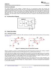
Overview (continued)
The output frequency of the oscillator is divided down by an asynchronous divider that provides two
complementary output signals with a 50% duty cycle. A subsequent break-before-make logic inserts a dead-time
between the high-pulses of the two signals. The resulting output signals, present the gate-drive signals for the
output transistors. As shown in the functional block diagram, before either one of the gates can assume logic
high, there must be a short time period during which both signals are low and both transistors are high-
impedance. This short period, known as break-before-make time, is required to avoid shorting out both ends of
the primary.
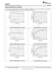
8.2 Functional Block Diagram
8.3 Feature Description
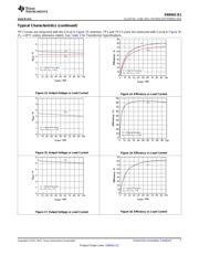
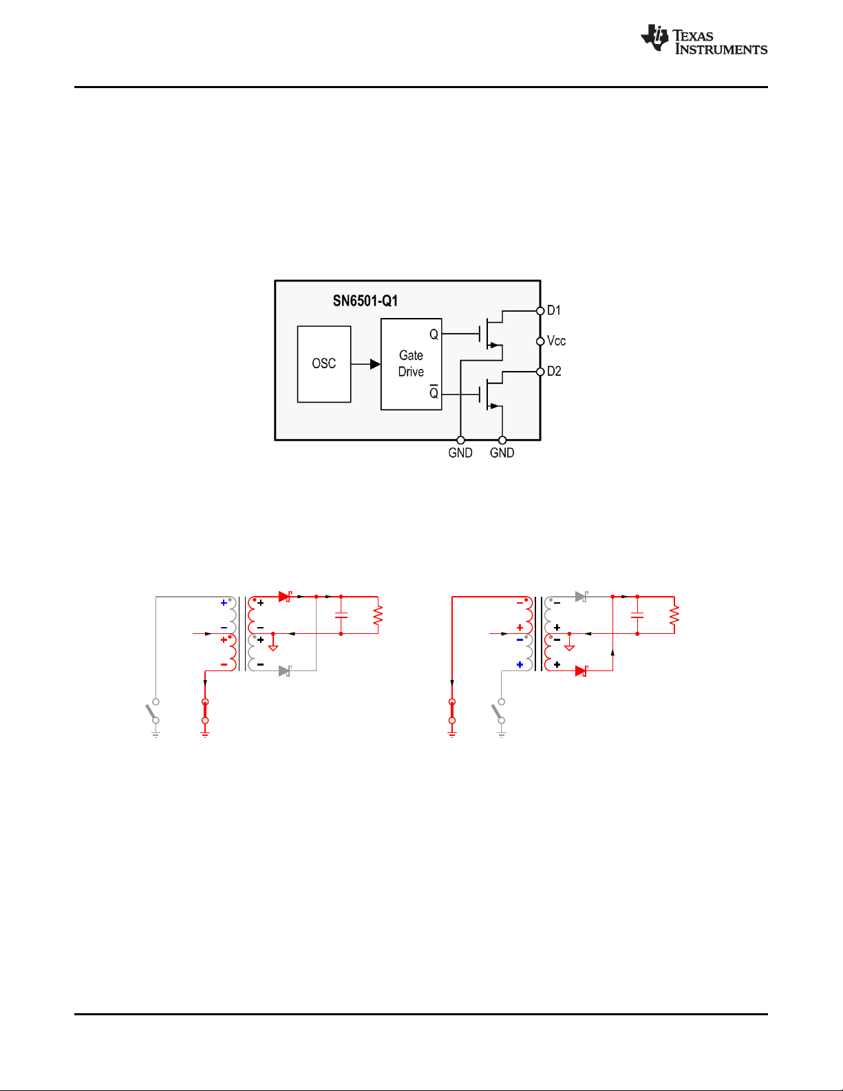
8.3.1 Push-Pull Converter
Push-pull converters require transformers with center-taps to transfer power from the primary to the secondary
(see Figure 37).
Figure 37. Switching Cycles of a Push-Pull Converter
When Q
1
conducts, V
IN
drives a current through the lower half of the primary to ground, thus creating a negative
voltage potential at the lower primary end with regards to the V
IN
potential at the center-tap.
At the same time the voltage across the upper half of the primary is such that the upper primary end is positive
with regards to the center-tap in order to maintain the previously established current flow through Q
2
, which now
has turned high-impedance. The two voltage sources, each of which equaling V
IN
, appear in series and cause a
voltage potential at the open end of the primary of 2×V
IN
with regards to ground.
Per dot convention the same voltage polarities that occur at the primary also occur at the secondary. The
positive potential of the upper secondary end therefore forward biases diode CR
1
. The secondary current starting
from the upper secondary end flows through CR
1
, charges capacitor C, and returns through the load impedance
R
L
back to the center-tap.
12 Submit Documentation Feedback Copyright © 2013–2014, Texas Instruments Incorporated
Product Folder Links: SN6501-Q1
器件 Datasheet 文档搜索
AiEMA 数据库涵盖高达 72,405,303 个元件的数据手册,每天更新 5,000 多个 PDF 文件
