Datasheet 搜索 > 接口芯片 > TI(德州仪器) > SN65HVD12PG4 数据手册 > SN65HVD12PG4 数据手册 1/36 页

¥ 23.063
SN65HVD12PG4 数据手册 - TI(德州仪器)
制造商:
TI(德州仪器)
分类:
接口芯片
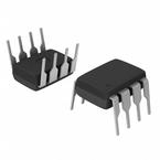
封装:
DIP-8
Pictures:
3D模型
符号图
焊盘图
引脚图
产品图
页面导航:
引脚图在P3Hot
典型应用电路图在P1P20P21
原理图在P16P17
封装尺寸在P28P29P30P32P33
标记信息在P3P28P29P30
封装信息在P27P28P29P30P31P32P33
技术参数、封装参数在P4
应用领域在P1P31
电气规格在P5P6P21
型号编号列表在P3
导航目录
SN65HVD12PG4数据手册
Page:
of 36 Go
若手册格式错乱,请下载阅览PDF原文件
R
T
R
T
R
A B
R RE DE D
D
R
A B
R RE DE D
D
R
D
R
RE
DE
D
A
B
R
D
R
RE
DE
D
A
B
Copyright © 2016, Texas Instruments Incorporated
Product
Folder
Order
Now
Technical
Documents
Tools &
Software
Support &
Community
An IMPORTANT NOTICE at the end of this data sheet addresses availability, warranty, changes, use in safety-critical applications,
intellectual property matters and other important disclaimers. PRODUCTION DATA.
SN65HVD10
,
SN65HVD10Q
,
SN75HVD10
,
SN65HVD11
SN65HVD12
,
SN75HVD12
,
SN65HVD11Q
,
SN75HVD11
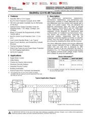
SLLS505O –FEBRUARY 2002–REVISED FEBRUARY 2017
SNx5HVD1x 3.3-V RS-485 Transceivers
1
(1) The signaling rate of a line is the number of voltage
transitions that are made per second expressed in the units
bps (bits per second).
1 Features
1
• Operates With a 3.3-V Supply
• Bus-Pin ESD Protection Exceeds 16-kV HBM
• 1/8 Unit-Load Option Available (Up to 256 Nodes
on the Bus)
• Optional Driver Output Transition Times for
Signaling Rates
(1)
of 1 Mbps, 10 Mbps, and
32 Mbps
• Meets or Exceeds the Requirements of ANSI
TIA/EIA-485-A
• Bus-Pin Short-Circuit Protection From –7 V to
12 V
• Low-Current Standby Mode: 1 µA, Typical
• Open-Circuit, Idle-Bus, and Shorted-Bus Failsafe
Receiver
• Thermal Shutdown Protection
• Glitch-Free Power-Up and Power-Down Protection
for Hot-Plugging Applications
• SN75176 Footprint
2 Applications
• Digital Motor Control
• Utility Meters
• Chassis-to-Chassis Interconnects
• Electronic Security Stations
• Industrial Process Control
• Building Automation
• Point-of-Sale (POS) Terminals and Networks
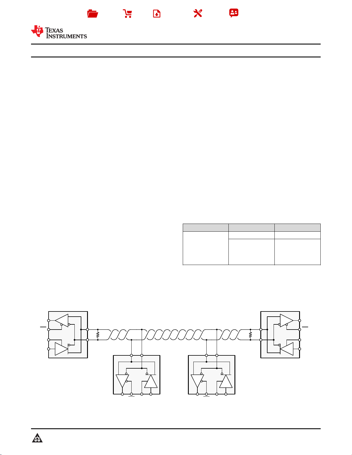
3 Description
The SN65HVD10, SN75HVD10, SN65HVD11,
SN75HVD11, SN65HVD12, and SN75HVD12 bus
transceivers combine a 3-state differential line driver
and differential input line receiver that operate with a
single 3.3-V power supply. They are designed for
balanced transmission lines and meet or exceed
ANSI standard TIA/EIA-485-A and ISO 8482:1993.
These differential bus transceivers are monolithic
integrated circuits designed for bidirectional data
communication on multipoint bus-transmission lines.
The drivers and receivers have active-high and
active-low enables, respectively, that can be
externally connected together to function as direction
control. Very low device standby supply current can
be achieved by disabling the driver and the receiver.
The driver differential outputs and receiver differential
inputs connect internally to form a differential input/
output (I/O) bus port that is designed to offer
minimum loading to the bus whenever the driver is
disabled or V
CC
= 0. These parts feature wide positive
and negative common-mode voltage ranges making
them suitable for party-line applications.
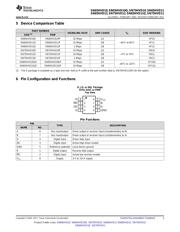
Device Information
(1)
PART NUMBER PACKAGE BODY SIZE (NOM)
SN65HVD12
SN75HVD12
SN65HVD11
SN75HVD12
SN65HVD10
SN75HVD10
SOIC (8) 4.90 mm × 3.91 mm
PDIP (8) 9.81 mm × 6.35 mm
(1) For all available packages, see the orderable addendum at
the end of the data sheet.
Typical Application Diagram
器件 Datasheet 文档搜索
AiEMA 数据库涵盖高达 72,405,303 个元件的数据手册,每天更新 5,000 多个 PDF 文件
