Datasheet 搜索 > CAN芯片 > TI(德州仪器) > SN65HVD233D 数据手册 > SN65HVD233D 数据手册 55/134 页
 器件3D模型
¥ 5.862
SN65HVD233D 数据手册 - TI(德州仪器)
制造商:
TI(德州仪器)
分类:
CAN芯片
封装:
SOIC-8
描述:
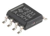
TEXAS INSTRUMENTS SN65HVD233D. 芯片, CAN总线收发器, 1MBPS, 1/1, 3.3V, SOIC-8
Pictures:
3D模型
符号图
焊盘图
引脚图
产品图
页面导航:
引脚图在P61P62P63Hot
典型应用电路图在P55
原理图在P31P46P50P51P54P56P57P58P66
封装尺寸在P128
标记信息在P128P129
封装信息在P5P110P128P129
应用领域在P134
型号编号列表在P67


导航目录
SN65HVD233D数据手册
Page:
of 134 Go
若手册格式错乱,请下载阅览PDF原文件

TMS320LF2407A,TMS320LF2406A,TMS320LF2403A,TMS320LF2402A
TMS320LC2406A,TMS320LC2404A,TMS320LC2403A,TMS320LC2402A
DSP CONTROLLERS
SPRS145L − JULY 2000 − REVISED SEPTEMBER 2007
55
POST OFFICE BOX 1443 • HOUSTON, TEXAS 77251−1443
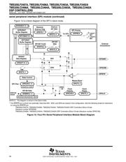
serial peripheral interface (SPI) module
Some 240xA devices include the four-pin serial peripheral interface (SPI) module. The SPI is a high-speed,
synchronous serial I/O port that allows a serial bit stream of programmed length (one to sixteen bits) to be shifted
into and out of the device at a programmable bit-transfer rate. Normally, the SPI is used for communications
between the DSP controller and external peripherals or another processor. Typical applications include external
I/O or peripheral expansion through devices such as shift registers, display drivers, and ADCs. Multidevice
communications are supported by the master/slave operation of the SPI.
The SPI module features include:
D Four external pins:
− SPISOMI: SPI slave-output/master-input pin
− SPISIMO: SPI slave-input/master-output pin
− SPISTE
: SPI slave transmit-enable pin
− SPICLK: SPI serial-clock pin
NOTE: All four pins can be used as GPIO, if the SPI module is not used.
D Two operational modes: master and slave
D Baud rate: 125 different programmable rates/10 Mbps at 40-MHz CPUCLK
D Data word length: one to sixteen data bits
D Four clocking schemes (controlled by clock polarity and clock phase bits) include:
− Falling edge without phase delay: SPICLK active high. SPI transmits data on the falling edge of the
SPICLK signal and receives data on the rising edge of the SPICLK signal.
− Falling edge with phase delay: SPICLK active high. SPI transmits data one half-cycle ahead of the
falling edge of the SPICLK signal and receives data on the falling edge of the SPICLK signal.
− Rising edge without phase delay: SPICLK inactive low. SPI transmits data on the rising edge of the
SPICLK signal and receives data on the falling edge of the SPICLK signal.
− Rising edge with phase delay: SPICLK inactive low. SPI transmits data one half-cycle ahead of the
falling edge of the SPICLK signal and receives data on the rising edge of the SPICLK signal.
D Simultaneous receive and transmit operation (transmit function can be disabled in software)
D Transmitter and receiver operations are accomplished through either interrupt-driven or polled algorithms.
D Nine SPI module control registers: Located in control register frame beginning at address 7040h.
NOTE: All registers in this module are 16-bit registers that are connected to the 16-bit peripheral bus. When a register is accessed, the
register data is in the lower byte (7 −0), and the upper byte (15 − 8) is read as zeros. Writing to the upper byte has no effect.
器件 Datasheet 文档搜索
AiEMA 数据库涵盖高达 72,405,303 个元件的数据手册,每天更新 5,000 多个 PDF 文件
