Datasheet 搜索 > 接口芯片 > TI(德州仪器) > SN65HVD3082EDG4 数据手册 > SN65HVD3082EDG4 数据手册 1/21 页
 器件3D模型
¥ 7.35
SN65HVD3082EDG4 数据手册 - TI(德州仪器)
制造商:
TI(德州仪器)
分类:
接口芯片
封装:
SOIC-8
描述:
低功耗RS - 485收发器,可在小型MSOP- 8封装 Low-Power RS-485 Transceivers, Available in a Small MSOP-8 Package
Pictures:
3D模型
符号图
焊盘图
引脚图
产品图
页面导航:
引脚图在P2Hot
原理图在P1
封装尺寸在P2P16P17P18
型号编码规则在P2
标记信息在P2
封装信息在P2P16P17P18
功能描述在P3
技术参数、封装参数在P7
应用领域在P1P21
电气规格在P8P9P10
导航目录
SN65HVD3082EDG4数据手册
Page:
of 21 Go
若手册格式错乱,请下载阅览PDF原文件
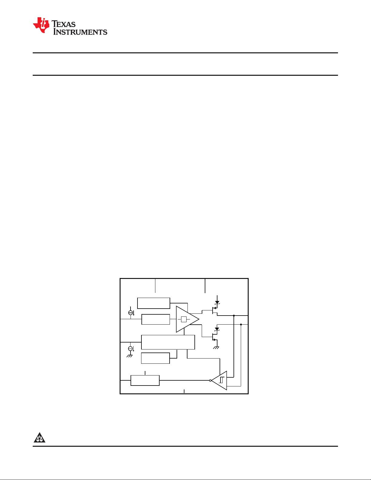
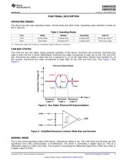
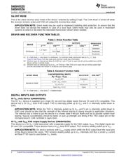
V
CC
CANH
7
6
CANL
RXD
1
TXD
S
8
DOMINANT
TIME OUT
OVER
TEMPERATURE
LOGIC
OUTPUT
MODE SELECT
4
NC / V
RXD
(See Note A)
V
CC
5 3
GND
2
UNDER
VOLTAGE
V
CC
V
CC
or V
RXD
(See Note B)
SN65HVD255
SN65HVD256
www.ti.com
SLLSEA2 –DECEMBER 2011
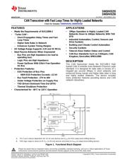
CAN Transceiver with Fast Loop Times for Highly Loaded Networks
Check for Samples: SN65HVD255, SN65HVD256
1
FEATURES
APPLICATIONS
• Meets the Requirements of ISO11898-2 • 1Mbps Operation in Highly Loaded CAN
Networks Down to 10kbps Networks With TXD
• “ Turbo CAN” :
DTO
– Short Propagation Delay Times and Fast
• Industrial Automation, Control, Sensors and
Loop Times
Drive Systems
– Higher Data Rates in Network
• Building and Climate Control Automation
– Enhances System Timing Margins
• Security Systems
• I/O Voltage Range Supports 3.3V and 5V MCUs
• Telecom Base Station Status and Control
• Ideal Passive Behavior When Unpowered
• CAN Bus Standards Such as CANopen, CAN
– Bus Pins are High Impedance (no load to
Kingdom, DeviceNet, NMEA2000
operating bus)
– Logic Pins are High Impedance
DESCRIPTION
– Power Up/Down With Glitch Free Operation
This CAN transceiver meets the ISO1189-2 High
On Bus
Speed CAN (Controller Area Network) Physical Layer
standard. It is designed for data rates in excess of 1
• Protection Features:
megabit per second (Mbps) in short networks and
– ESD Protection of Bus Pins
enhanced timing margin and higher data rates in long
– HBM ESD Protection Exceeds ±12 kV
and highly loaded networks. The device includes
– Bus Fault Protection –27V to 40V
many protection features providing device and CAN
network robustness.
– Under Voltage Protection on Supply Pins
– TXD (Driver) Dominant Time Out (DTO)
– Thermal Shutdown Protection
• Characterized for –40°C to 125°C Operation
A. Pin 5 use is device dependent. NC for 5V-only devices and V
RXD
for RXD output level-shifting devices.
B. RXD logic output is driven to 5V V
CC
on 5V-only devices and driven to V
RXD
on output level-shifting devices.
Figure 1. Functional Block Diagram
1
Please be aware that an important notice concerning availability, standard warranty, and use in critical applications of Texas
Instruments semiconductor products and disclaimers thereto appears at the end of this data sheet.
PRODUCTION DATA information is current as of publication date.
Copyright © 2011, Texas Instruments Incorporated
Products conform to specifications per the terms of the Texas
Instruments standard warranty. Production processing does not
necessarily include testing of all parameters.
器件 Datasheet 文档搜索
AiEMA 数据库涵盖高达 72,405,303 个元件的数据手册,每天更新 5,000 多个 PDF 文件
