Datasheet 搜索 > RS485控制器 > TI(德州仪器) > SN65HVD72DRBR 数据手册 > SN65HVD72DRBR 数据手册 5/39 页
 器件3D模型
¥ 6.711
SN65HVD72DRBR 数据手册 - TI(德州仪器)
制造商:
TI(德州仪器)
分类:
RS485控制器
封装:
VDFN-8
描述:
RS-485接口IC 3.3V-Supply RS-485 w/ IEC ESD Protect
Pictures:
3D模型
符号图
焊盘图
引脚图
产品图
页面导航:
引脚图在P4Hot
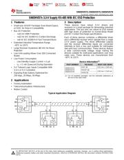
典型应用电路图在P1P16P18P19
原理图在P15
封装尺寸在P28P29P30P31
标记信息在P28P29
封装信息在P27P28P29P30P31
技术参数、封装参数在P5
应用领域在P1P39
电气规格在P6P7P19
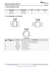
型号编号列表在P4
导航目录
SN65HVD72DRBR数据手册
Page:
of 39 Go
若手册格式错乱,请下载阅览PDF原文件
SN65HVD72
,
SN65HVD75
,
SN65HVD78
www.ti.com
SLLSE11D –MARCH 2012–REVISED JULY 2015
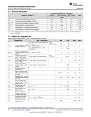
7 Specifications
7.1 Absolute Maximum Ratings
over recommended operating range (unless otherwise specified)
(1)
MIN MAX UNIT
Supply voltage, V
CC
–0.5 5.5
Voltage at A or B inputs –13 16.5
V
Input voltage at any logic pin –0.3 5.7
Voltage input, transient pulse, A and B, through 100 Ω –100 100
Receiver output current –24 24 mA
Junction temperature, T
J
170 °C
Continuous total power dissipation See Power Dissipation
Storage temperature, T
stg
–65 150 °C
(1) Stresses beyond those listed under Absolute Maximum Ratings may cause permanent damage to the device. These are stress ratings
only and functional operation of the device at these or any other conditions beyond those indicated under Recommended Operating
Conditions is not implied. Exposure to absolute-maximum-rated conditions for extended periods may affect device reliability.
7.2 ESD Ratings
VALUE UNIT
Human body model (HBM), per ANSI/ESDA/JEDEC JS-001, all pins
(1)
±8000
Charged device model (CDM), per JEDEC specification JESD22-C101, all ±1500
pins
(2)
JEDEC Standard 22, Test Method A115 (Machine Model), all pins ±300
Electrostatic
V
(ESD)
V
discharge IEC 61000-4-2 ESD (Air-Gap Discharge), bus pins and GND
(3)
±12000
IEC 61000-4-2 ESD (Contact Discharge), bus pins and GND ±12000
IEC 61000-4-4 EFT (Fast transient or burst) bus pins and GND ±4000
IEC 60749-26 ESD (Human Body Model), bus pins and GND ±15000
(1) JEDEC document JEP155 states that 500-V HBM allows safe manufacturing with a standard ESD control process.
(2) JEDEC document JEP157 states that 250-V CDM allows safe manufacturing with a standard ESD control process.
(3) By inference from contact discharge results, see Application and Implementation.
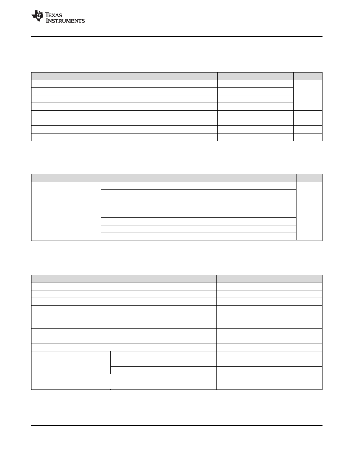
7.3 Recommended Operating Conditions
MIN NOM MAX UNIT
V
CC
Supply voltage 3 3.3 3.6 V
V
I
Input voltage at any bus terminal (separately or common mode)
(1)
–7 12 V
V
IH
High-level input voltage (driver, driver enable, and receiver enable inputs) 2 V
CC
V
V
IL
Low-level input voltage (driver, driver enable, and receiver enable inputs) 0 0.8 V
V
ID
Differential input voltage –12 12 V
I
O
Output current, driver –60 60 mA
I
O
Output current, receiver –8 8 mA
R
L
Differential load resistance 54 60 Ω
C
L
Differential load capacitance 50 pF
SN65HVD72 250 kbps
1/t
UI
Signaling rate SN65HVD75 20 Mbps
SN65HVD78 50 Mbps
T
A
(2)
Operating free-air temperature (See Thermal Information) –40 125 °C
T
J
Junction temperature –40 150 °C
(1) The algebraic convention, in which the least positive (most negative) limit is designated as minimum, is used in this data sheet.
(2) Operation is specified for internal (junction) temperatures up to 150°C. Self-heating due to internal power dissipation should be
considered for each application. Maximum junction temperature is internally limited by the thermal shutdown (TSD) circuit which disables
the driver outputs when the junction temperature reaches 170°C.
Copyright © 2012–2015, Texas Instruments Incorporated Submit Documentation Feedback 5
Product Folder Links: SN65HVD72 SN65HVD75 SN65HVD78
器件 Datasheet 文档搜索
AiEMA 数据库涵盖高达 72,405,303 个元件的数据手册,每天更新 5,000 多个 PDF 文件
