Datasheet 搜索 > 接口芯片 > TI(德州仪器) > SN65LVDS048ADRG4 数据手册 > SN65LVDS048ADRG4 数据手册 3/13 页
 器件3D模型
¥ 19.205
SN65LVDS048ADRG4 数据手册 - TI(德州仪器)
制造商:
TI(德州仪器)
分类:
接口芯片
封装:
SOIC-16
描述:
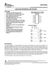
LVDS四路差动线路接收器 LVDS QUAD DIFFERENTIAL LINE RECEIVER
Pictures:
3D模型
符号图
焊盘图
引脚图
产品图
页面导航:
导航目录
SN65LVDS048ADRG4数据手册
Page:
of 13 Go
若手册格式错乱,请下载阅览PDF原文件
www.ti.com
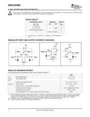
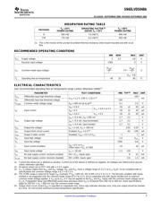
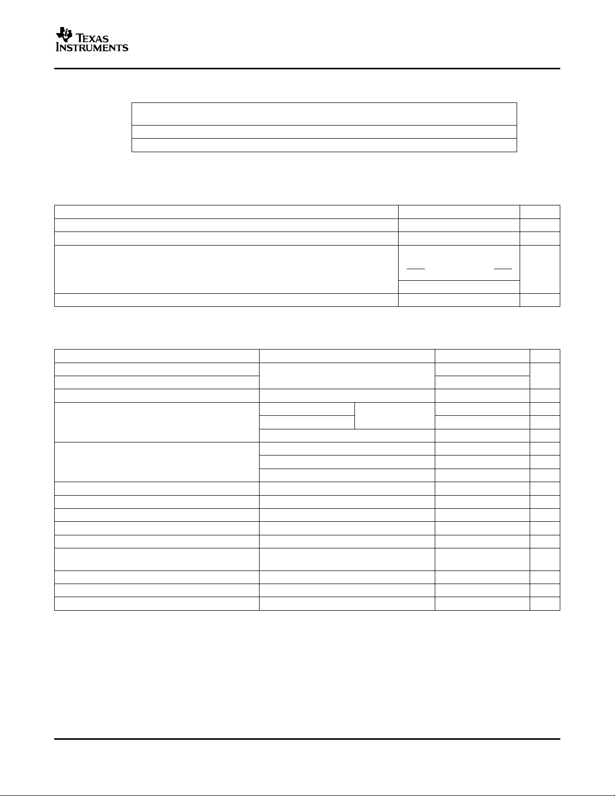
DISSIPATION RATING TABLE
RECOMMENDED OPERATING CONDITIONS
|V
ID
|
2
2.4
|V
ID
|
2
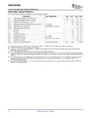
ELECTRICAL CHARACTERISTICS
SN65LVDS048A
SLLS451B – SEPTEMBER 2000 – REVISED SEPTEMBER 2002
T
A
≤ 25°C OPERATING FACTOR
(1)
T
A
= 85°C
PACKAGE
POWER RATING ABOVE T
A
= 25°C POWER RATING
D 950 mW 7.6 mW/°C 494 mW
PW 774 mW 6.2 mW/°C 402 mW
(1) This is the inverse of the junction-to-ambient thermal resistance when board-mounted and with no air
flow.
MIN NOM MAX UNIT
V
CC
Supply voltage 3 3.3 3.6 V
Receiver input voltage GND 3 V
V
IC
Common-mode input voltage V
V
CC
– 0.8
T
A
Operating free-air temperature –40 25 85 °C
over recommended operating free-air temperature range (unless otherwise noted)
(1)
PARAMETER TEST CONDITIONS MIN TYP
(2)
MAX UNIT
V
IT+
Differential input high threshold voltage 100
V
CM
= 1.2 V, 0.05 V, 2.35 V
(3)
mV
V
IT–
Differential input low threshold voltage –100
V
(CMR)
Common mode voltage range V
ID
= 200 mV pk to pk
(4)
0.1 2.3 V
V
IN
= 2.8 V –20 ±1 20 µA
V
CC
= 3.6 V or 0 V
I
IN
Input current V
IN
= 0 V –20 ±1 20 µA
V
IN
= 3.6 V, V
CC
= 0 V –20 ±1 20 µA
I
OH
= -0.4 mA, V
ID
= 200 mV 2.7 3.2 V
V
OH
Output high voltage I
OH
= -0.4 mA, input terminated 2.7 3.2 V
I
OH
= -0.4 mA, input shorted 2.7 3.2 V
V
OL
Output low voltage I
OL
= 2 mA, V
ID
= -200 mV 0.05 0.25 V
I
OS
Output short circuit current Enabled, V
OUT
= 0 V
(5)
–65 –100 mA
I
O(Z)
Output 3-state current Disabled, V
OUT
= 0 V or V
CC
–1 1 µA
V
IH
Input high voltage 2.0 V
CC
V
V
IL
Input low voltage GND 0.8 V
V
IN
= 0 V or V
CC
,
I
I
Input current (enables) –10 10 µA
Other input = V
CC
or GND
V
IK
Input clamp voltage I
CL
= –18 mA –1.5 –0.8 V
I
CC
No load supply current, receivers enabled EN = V
CC
, Inputs open 8 15 mA
I
CC(Z)
No load supply current, receivers disabled EN = GND, Inputs open 0.6 1.5 mA
(1) Current into device pin is defined as positive. Current out of the device is defined as negative. All voltages are referenced to ground,
unless otherwise specified.
(2) All typical values are at 25°C and with a 3.3-V supply.
(3) V
CC
is always higher than R
IN+
and R
IN-
voltage, R
IN-
and R
IN+
have a voltage range of -0.2 V to V
CC
-V
ID
/2. To be compliant with ac
specifications the common voltage range is 0.1 V to 2.3 V.
(4) The VCMR range is reduced for larger V
ID
, Example: If V
ID
= 400 mV, the VCMR is 0.2 V to 2.2 V. The fail-safe condition with inputs
shorted is not supported over the common-mode range of 0 V to 2.4 V, but is supported only with inputs shorted and no external
common-mode voltage applied. A V
ID
up to V
CC
-0 V may be applied to the R
IN+
and R
IN-
inputs with the common-mode voltage set to
V
CC
/2. Propagation delay and differential pulse skew decrease when V
ID
is increased from 200 mV to 400 mV. Skew specifications
apply for 200 mV < V
ID
< 800 mV over the common-mode range.
(5) Output short circuit current (I
OS
) is specified as magnitude only, minus sign indicates direction only. Only one output should be shorted
at a time. Do not exceed maximum junction temperature specification.
3
Submit Documentation Feedback
器件 Datasheet 文档搜索
AiEMA 数据库涵盖高达 72,405,303 个元件的数据手册,每天更新 5,000 多个 PDF 文件
