Datasheet 搜索 > 接口芯片 > TI(德州仪器) > SN65LVDS048PW 数据手册 > SN65LVDS048PW 数据手册 3/13 页
 器件3D模型
¥ 4.974
SN65LVDS048PW 数据手册 - TI(德州仪器)
制造商:
TI(德州仪器)
分类:
接口芯片
封装:
TSSOP
描述:
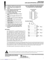
LVDS四路差动线路接收器 LVDS QUAD DIFFERENTIAL LINE RECEIVER
Pictures:
3D模型
符号图
焊盘图
引脚图
产品图
页面导航:
封装尺寸在P12
封装信息在P12
应用领域在P13
导航目录
SN65LVDS048PW数据手册
Page:
of 13 Go
若手册格式错乱,请下载阅览PDF原文件
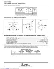
SN65LVDS048
LVDS QUAD DIFFERENTIAL LINE RECEIVER
SLLS415A – JUNE 2000 – REVISED SEPTEMBER 2000
3
POST OFFICE BOX 655303 • DALLAS, TEXAS 75265
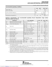
recommended operating conditions
MIN NOM MAX UNIT
Supply voltage, V
CC
3 3.3 3.6 V
Receiver input voltage GND 3 V
Common–mode input voltage, V
IC
|V
ID
|
2
2.4
*
|V
ID
|
2
V
V
CC
– 0.8
Operating free-air temperature, T
A
–40 25 85 °C
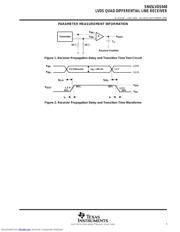
electrical characteristics over recommended operating free-air temperature range (unless
otherwise noted) (see Note 2)
PARAMETER TEST CONDITIONS MIN TYP
†
MAX UNIT
V
IT+
Differential input high threshold voltage
V
CM
= 1.2 V, 0.05 V, 2.35 V
100
mV
V
IT–
Differential input low threshold voltage
CM
,,
(see Note 3)
–100
mV
V
(CMR)
Common mode voltage range V
ID
= 200 mV pk to pk (see Note 4) 0.1 2.3 V
V
IN
= 2.8 V
V
CC
=36Vor0V
–20 ±1 20 µA
I
IN
Input current
V
IN
= 0 V
V
CC
=
3
.
6
V
or
0
V
–20 ±1 20 µA
V
IN
= 3.6 V V
CC
= 0 V –20 ±1 20 µA
I
OH
= –0.4 mA, V
ID
= 200 mV 2.7 3.2 V
V
OH
Output high voltage
I
OH
= –0.4 mA, input terminated
2.7 3.2 V
I
OH
= –0.4 mA, input shorted 2.7 3.2 V
V
OL
Output low voltage I
OL
= 2 mA, V
ID
= –200 mV 0.05 0.25 V
I
OS
Output short circuit current Enabled, V
OUT
= 0 V (see Note 5) –65 –100 mA
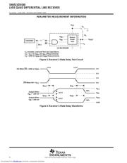
I
O(Z)
Output 3-state current Disabled, V
OUT
= 0 V or V
CC
–1 1 µA
V
IH
Input high voltage 2.0 V
CC
V
V
IL
Input low voltage GND 0.8 V
I
I
Input current (enables)
V
IN
= 0 V or V
CC
,
Other input = V
CC
or GND
–10 10 µA
V
IK
Input clamp voltage I
CL
= –18 mA –1.5 –0.8 V
I
CC
No load supply current, receivers enabled EN = V
CC
, Inputs open 8 15 mA
I
CC(Z)
No load supply current, receivers disabled EN = GND, Inputs open 0.6 1.5 mA
†
All typical values are at 25°C and with a 3.3-V supply.
NOTES: 2. Current into device pin is defined as positive. Current out of the device is defined as negative. All voltages are referenced to ground,
unless otherwise specified.
3. V
CC
is always higher than R
IN+
and R
IN–
voltage, R
IN–
and R
IN+
have a voltage range of –0.2 V to V
CC
–V
ID
/2. To be compliant with
ac specifications the common voltage range is 0.1 V to 2.3 V.
4. The VCMR range is reduced for larger V
ID
, Example: If V
ID
= 400 mV, the VCMR is 0.2 V to 2.2 V. The fail-safe condition with inputs
shorted is not supported over the common-mode range of 0 V to 2.4 V, but is supported only with inputs shorted and no external
common-mode voltage applied. A V
ID
up to V
CC
–0 V may be applied to the R
IN+
and R
IN–
inputs with the common-mode voltage
set to V
CC
/2. Propagation delay and differential pulse skew decrease when V
ID
is increased from 200 mV to 400 mV. Skew
specifications apply for 200 mV < V
ID
< 800 mV over the common-mode range.
5. Output short circuit current (I
OS
) is specified as magnitude only, minus sign indicates direction only. Only one output should be
shorted at a time. Do not exceed maximum junction temperature specification.
Downloaded from Elcodis.com electronic components distributor
器件 Datasheet 文档搜索
AiEMA 数据库涵盖高达 72,405,303 个元件的数据手册,每天更新 5,000 多个 PDF 文件
