Datasheet 搜索 > 逻辑控制器 > TI(德州仪器) > SN65LVDT250DBT 数据手册 > SN65LVDT250DBT 数据手册 1/20 页
 器件3D模型
¥ 104.375
SN65LVDT250DBT 数据手册 - TI(德州仪器)
制造商:
TI(德州仪器)
分类:
逻辑控制器
封装:
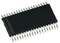
TSSOP-38
描述:
DS25CP104A,4X4 3.125 Gbps LVDS 交叉点开关,Texas Instruments### 开关和多路复用器,Texas Instruments信号开关和多路复用器实现连接器共享,最大程度减少了设计内的重复电路。 它们还隔离信号路径并简化信号布线。
Pictures:
3D模型
符号图
焊盘图
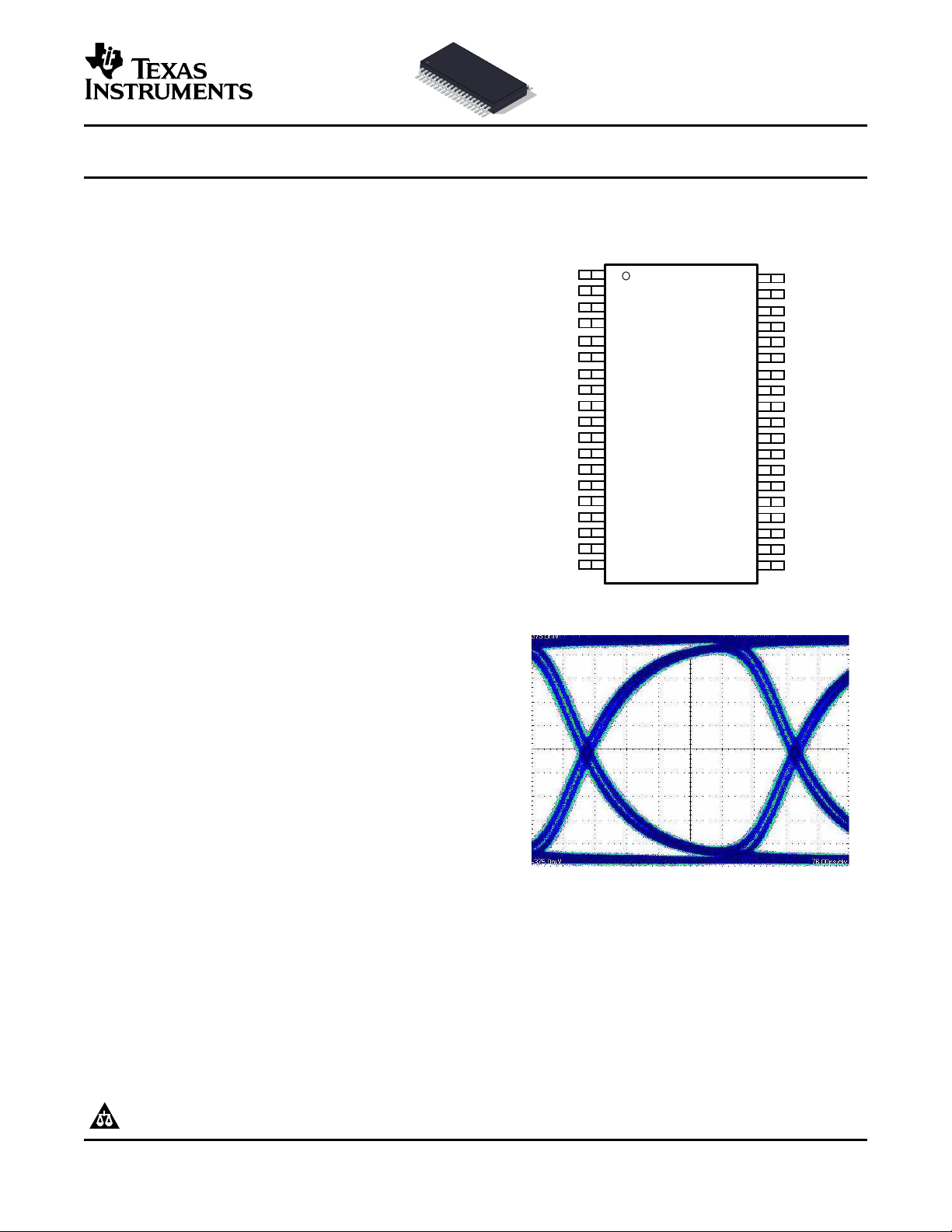
引脚图
产品图
页面导航:

导航目录
SN65LVDT250DBT数据手册
Page:
of 20 Go
若手册格式错乱,请下载阅览PDF原文件
www.ti.com
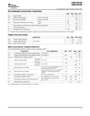
FEATURES
1
2
3
4
5
6
7
8
9
10
11
12
13
14
15
16
17
18
19
38
37
36
35
34
33
32
31
30
29
28
27
26
25
24
23
22
21
20
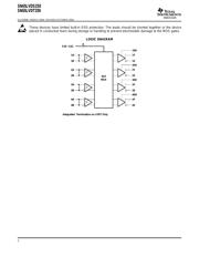
S10
S11
1A
1B
S20
S21
2A
2B
GND
VCC
GND
3A
3B
S30
S31
4A
4B
S40
S41
VCC
GND
1Y
1Z
1DE
2Y
2Z
2DE
GND
VCC
GND
3Y
3Z
3DE
4Y
4Z
4DE
GND
VCC
SN65LVDS250DBT ( Marked as LVDS250)
SN65LVDT250DBT ( Marked as LVDT250)
(TOP VIEW)
APPLICATIONS
DESCRIPTION
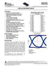
76 − ps/div
75 mV/div
V
IC
= 1.2 V
|V
ID
| = 200 mV
2 Gbps
Input = PRBS 2
23
−1
V
CC
= 3.3 V
SN65LVDS250
SN65LVDT250
SLLS594B – MARCH 2004 – REVISED OCTOBER 2004
LVDS 4x4 CROSSPOINT SWITCH
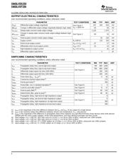
• Greater Than 2.0 Gbps Operation
• Nonblocking Architecture Allows Each
Output to be Connected to Any Input
• Pk-Pk Jitter:
– 60 ps Typical at 2.0 Gbps
– 110 ps Typical at 2.5 Gbps
• Compatible With ANSI TIA/EIA-644-A LVDS
Standard
• Available Packaging 38-Pin TSSOP
• 25 mV of Input Voltage Threshold Hysteresis
• Propagation Delay Times: 800 ps Typical
• Inputs Electrically Compatible With LVPECL,
CML and LVDS Signal Levels
• Operates From a Single 3.3-V Supply
• Low Power: 110 mA Typical
• Integrated 110- Ω Line Termination Resistors
Available With SN65LVDT250
EYE PATTERN
• Clock Buffering/Clock Muxing
• Wireless Base Stations
• High-Speed Network Routing
• Telecom/Datacom
The SN65LVDS250 and SN65LVDT250 are 4x4
nonblocking crosspoint switches in a flow-through
pin-out allowing for ease in PCB layout. Low-voltage
differential signaling (LVDS) is used to achieve a
high-speed data throughput while using low power.
Each of the output drivers includes a 4:1 multiplexer
to allow any input to be routed to any output. Internal
signal paths are fully differential to achieve the high
signaling speeds while maintaining low signal skews.
The SN65LVDT250 incorporates 110- Ω termination
resistors for those applications where board space is
a premium.
The SN65LVDS250 and SN65LVDT250 are
characterized for operation from -40 ° C to 85 ° C.
Please be aware that an important notice concerning availability, standard warranty, and use in critical applications of Texas
Instruments semiconductor products and disclaimers thereto appears at the end of this data sheet.
PRODUCTION DATA information is current as of publication date.
Copyright © 2004, Texas Instruments Incorporated
Products conform to specifications per the terms of the Texas
Instruments standard warranty. Production processing does not
necessarily include testing of all parameters.
器件 Datasheet 文档搜索
AiEMA 数据库涵盖高达 72,405,303 个元件的数据手册,每天更新 5,000 多个 PDF 文件
