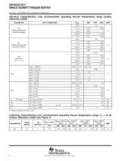
Datasheet 搜索 > 逻辑控制器 > TI(德州仪器) > SN74AUC1G17YEAR 数据手册 > SN74AUC1G17YEAR 数据手册 1/13 页
 器件3D模型
¥ 1.671
SN74AUC1G17YEAR 数据手册 - TI(德州仪器)
制造商:
TI(德州仪器)
分类:
逻辑控制器
封装:
DSBGA-5
描述:
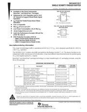
单施密特触发器缓冲 SINGLE SCHMITT TRIGGER BUFFER
Pictures:
3D模型
符号图
焊盘图
引脚图
产品图
页面导航:
导航目录
SN74AUC1G17YEAR数据手册
Page:
of 13 Go
若手册格式错乱,请下载阅览PDF原文件
SCES376J − SEPTEMBER 2001 − REVISED OCTOBER 2003
1
POST OFFICE BOX 655303 • DALLAS, TEXAS 75265
D Available in the Texas Instruments
NanoStar and NanoFree Packages
D Optimized for 1.8-V Operation and Is 3.6-V
I/O Tolerant to Support Mixed-Mode Signal
Operation
D I
off
Supports Partial-Power-Down Mode
Operation
D Sub 1-V Operable
D Max t
pd
of 2.4 ns at 1.8 V
D Low Power Consumption, 10-µA Max I
CC
D ±8-mA Output Drive at 1.8 V
D Latch-Up Performance Exceeds 100 mA Per
JESD 78, Class II
D ESD Protection Exceeds JESD 22
− 2000-V Human-Body Model (A114-A)
− 200-V Machine Model (A115-A)
− 1000-V Charged-Device Model (C101)
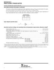
description/ordering information
This single Schmitt-trigger buffer is operational at 0.8-V to 2.7-V V
CC
, but is designed specifically for 1.65-V to
1.95-V V
CC
operation.
The SN74AUC1G17 contains one buffer and performs the Boolean function Y = A. The device functions as an
independent buffer, but because of Schmitt action, it may have different input threshold levels for positive-going
(V
T+
) and negative-going (V
T−
) signals.
NanoStar and NanoFree package technology is a major breakthrough in IC packaging concepts, using the
die as the package.
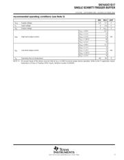
ORDERING INFORMATION
T
A
PACKAGE
†
ORDERABLE
PART NUMBER
TOP-SIDE
MARKING
‡
NanoStar − WCSP (DSBGA)
0.17-mm Small Bump − YEA
SN74AUC1G17YEAR
NanoFree − WCSP (DSBGA)
0.17-mm Small Bump − YZA (Pb-free)
Tape and reel
SN74AUC1G17YZAR
_ _ _U7_
−40°C to 85°C
NanoStar − WCSP (DSBGA)
0.23-mm Large Bump − YEP
Tape and reel
SN74AUC1G17YEPR
_ _ _U7_
NanoFree − WCSP (DSBGA)
0.23-mm Large Bump − YZP (Pb-free)
SN74AUC1G17YZPR
SOT (SOT-23) − DBV Tape and reel SN74AUC1G17DBVR U17_
SOT (SC-70) − DCK Tape and reel SN74AUC1G17DCKR U7_
†
Package drawings, standard packing quantities, thermal data, symbolization, and PCB design guidelines are available at
www.ti.com/sc/package.
‡
DBV/DCK: The actual top-side marking has one additional character that designates the assembly/test site.
YEA/YZA, YEP/YZP: The actual top-side marking has three preceding characters to denote year, month, and sequence code,
and one following character to designate the assembly/test site. Pin 1 identifier indicates solder-bump composition (1 = SnPb,
• = Pb-free).
Copyright 2003, Texas Instruments Incorporated
Please be aware that an important notice concerning availability, standard warranty, and use in critical applications of
Texas Instruments semiconductor products and disclaimers thereto appears at the end of this data sheet.
NanoStar and NanoFree are trademarks of Texas Instruments.
DBV OR DCK PACKAGE
(TOP VIEW)
1
2
3
5
4
NC
A
GND
V
CC
Y
NC − No internal connection
DNU − Do not use
3
2
1
4
5
GND
A
DNU
Y
V
CC
YEA, YEP, YZA, OR YZP PACKAGE
(BOTTOM VIEW)
!"# $"%&! '#(
'"! ! $#!! $# )# # #* "#
'' +,( '"! $!#- '# #!#&, !&"'#
#- && $##(
器件 Datasheet 文档搜索
AiEMA 数据库涵盖高达 72,405,303 个元件的数据手册,每天更新 5,000 多个 PDF 文件
