Datasheet 搜索 > 逻辑控制器 > TI(德州仪器) > SN74AVC1T45DBVTG4 数据手册 > SN74AVC1T45DBVTG4 数据手册 14/34 页

¥ 2.758
SN74AVC1T45DBVTG4 数据手册 - TI(德州仪器)
制造商:
TI(德州仪器)
分类:
逻辑控制器
封装:
SOT-23-6
描述:
可配置电压转换和3态输出的单位双电源总线收发器 SINGLE-BIT DUAL-SUPPLY BUS TRANSCEIVER WITH CONFIGURABLE VOLTAGE TRANSLATION AND 3-STATE OUTPUTS
Pictures:
3D模型
符号图
焊盘图
引脚图
产品图
页面导航:
引脚图在P3Hot
典型应用电路图在P1P14
原理图在P13
封装尺寸在P21P23P24P31
焊盘布局在P32
标记信息在P21P22
封装信息在P3P20P21P22P23P24
功能描述在P14
技术参数、封装参数在P4
应用领域在P1P14
电气规格在P6
导航目录
SN74AVC1T45DBVTG4数据手册
Page:
of 34 Go
若手册格式错乱,请下载阅览PDF原文件
1
2
3
6
5
4
V
CC1
V
CC1
V
CC2
V
CC2
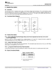
SYSTEM-1 SYSTEM-2
SN74AVC1T45
SCES530H –DECEMBER 2003–REVISED DECEMBER 2014
www.ti.com
10 Application and Implementation
NOTE
Information in the following applications sections is not part of the TI component
specification, and TI does not warrant its accuracy or completeness. TI’s customers are
responsible for determining suitability of components for their purposes. Customers should
validate and test their design implementation to confirm system functionality.
10.1 Application Information
The SN74AVC1T45 device can be used in level-translation applications for interfacing devices or systems
operating at different interface voltages with one another. The maximum data rate can be up to 500 Mbps when
device translate signal from 1.8 V to 3.3 V.
10.1.1 Enable Times
Calculate the enable times for the SN74AVC1T45 using the following formulas:
• t
PZH
(DIR to A) = t
PLZ
(DIR to B) + t
PLH
(B to A)
• t
PZL
(DIR to A) = t
PHZ
(DIR to B) + t
PHL
(B to A)
• t
PZH
(DIR to B) = t
PLZ
(DIR to A) + t
PLH
(A to B)
• t
PZL
(DIR to B) = t
PHZ
(DIR to A) + t
PHL
(A to B)
In a bidirectional application, these enable times provide the maximum delay from the time the DIR bit is
switched until an output is expected. For example, if the SN74AVC1T45 initially is transmitting from A to B, then
the DIR bit is switched; the B port of the device must be disabled before presenting it with an input. After the B
port has been disabled, an input signal applied to it appears on the corresponding A port after the specified
propagation delay.
10.2 Typical Applications
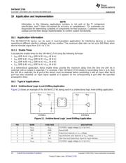
10.2.1 Unidirectional Logic Level-Shifting Application
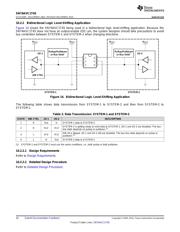
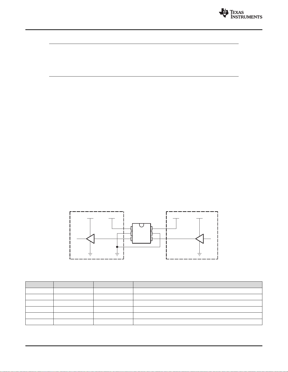
Figure 12 shows an example of the SN74AVC1T45 being used in a unidirectional logic level-shifting application.
Figure 12. Unidirectional Logic Level-Shifting Application
PIN NAME FUNCTION DESCRIPTION
1 V
CCA
V
CC1
SYSTEM-1 supply voltage (1.2 V to 3.6 V)
2 GND GND Device GND
3 A OUT Output level depends on V
CC1
voltage.
4 B IN Input threshold value depends on V
CC2
voltage.
5 DIR DIR GND (low level) determines B-port to A-port direction.
6 V
CCB
V
CC2
SYSTEM-2 supply voltage (1.2 V to 3.6 V)
14 Submit Documentation Feedback Copyright © 2003–2014, Texas Instruments Incorporated
Product Folder Links: SN74AVC1T45
器件 Datasheet 文档搜索
AiEMA 数据库涵盖高达 72,405,303 个元件的数据手册,每天更新 5,000 多个 PDF 文件
