Datasheet 搜索 > 电压电平转换器 > TI(德州仪器) > SN74AVCH4T245PWR 数据手册 > SN74AVCH4T245PWR 数据手册 1/24 页
 器件3D模型
¥ 3.064
SN74AVCH4T245PWR 数据手册 - TI(德州仪器)
制造商:
TI(德州仪器)
分类:
电压电平转换器
封装:
TSSOP-16
描述:
TEXAS INSTRUMENTS SN74AVCH4T245PWR 芯片, 收发器, 带电压转换器, 4位, TSSOP-16
Pictures:
3D模型
符号图
焊盘图
引脚图
产品图
页面导航:
典型应用电路图在P2
封装尺寸在P2P11P13P14
型号编码规则在P1P2
标记信息在P2P11P12
封装信息在P2P11P12P13P14
技术参数、封装参数在P3
应用领域在P12P24
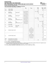
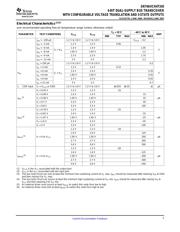
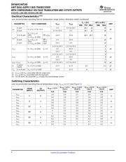
电气规格在P5P6
导航目录
SN74AVCH4T245PWR数据手册
Page:
of 24 Go
若手册格式错乱,请下载阅览PDF原文件
www.ti.com
FEATURES
1
2
3
4
5
6
7
8
16
15
14
13
12
11
10
9
V
CCA
1DIR
2DIR
1A1
1A2
2A1
2A2
GND
V
CCB
1OE
2OE
1B1
1B2
2B1
2B2
GND
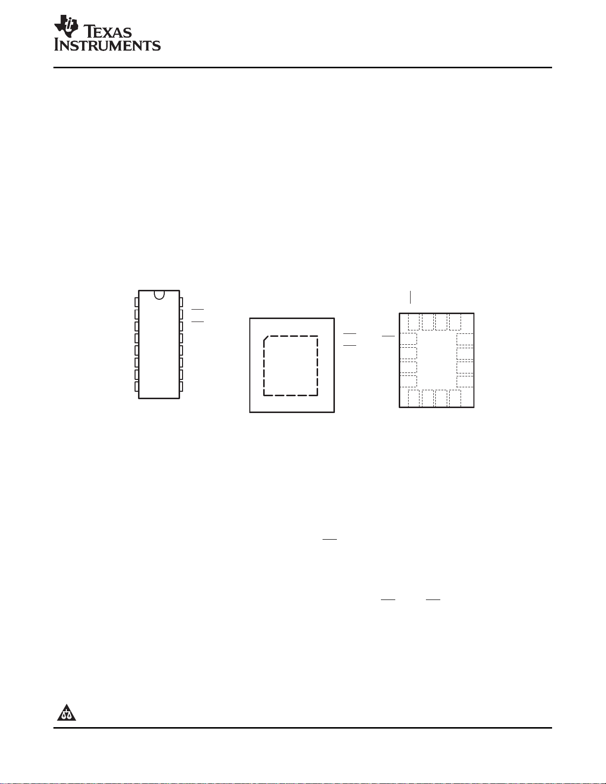
D, DGV, ORPWPACKAGE
(TOP VIEW)
RGYPACKAGE
(TOP VIEW)
RSVPACKAGE
(TOP VIEW)
1 16
8 9
2
3
4
5
6
7
15
14
13
12
11
10
1OE
2OE
1B1
1B2
2B1
2B2
1DIR
2DIR
1A1
1A2
2A1
2A2
GND
V
GND
CCB
V
CCA
1OE
2OE
1B1
1B2
2B1
2DIR
1A1
1A2
2A1
V
CCB
1DIR
V
CCA
4
3
2
1
2B2
2A2
GND
GND
11
10
9
12
16 15
14
13
5 6
7
8
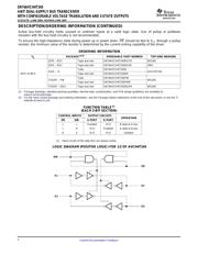
DESCRIPTION/ORDERING INFORMATION
SN74AVCH4T245
4-BIT DUAL-SUPPLY BUS TRANSCEIVER
WITH CONFIGURABLE VOLTAGE TRANSLATION AND 3-STATE OUTPUTS
SCES577D – JUNE 2004 – REVISED JUNE 2007
• Control Inputs V
IH
/V
IL
Levels Are Referenced • Max Data Rates
to V
CCA
Voltage
– 380 Mbps (1.8V to 3.3V Translation)
• Fully Configurable Dual-Rail Design Allows
– 200 Mbps (<1.8V to 3.3V Translation)
Each Port to Operate Over the Full 1.2-V to
– 200 Mbps (Translate to 2.5V or 1.8V)
3.6-V Power-Supply Range
– 150 Mbps (Translate to 1.5V)
• I/Os Are 4.6-V Tolerant
– 100 Mbps (Translate to 1.2V)
• I
off
Supports Partial Power-Down-Mode
• Latch-Up Performance Exceeds 100 mA Per
Operation
JESD 78, Class II
• Bus Hold on Data Inputs Eliminates the Need
• ESD Protection Exceeds JESD 22
for External Pullup/Pulldown Resistors
– 8000-V Human-Body Model (A114-A)
– 200-V Machine Model (A115-A)
– 1000-V Charged-Device Model (C101)
This 4-bit noninverting bus transceiver uses two separate configurable power-supply rails. The A port is
designed to track V
CCA
. V
CCA
accepts any supply voltage from 1.2 V to 3.6 V. The B port is designed to track
V
CCB
. V
CCB
accepts any supply voltage from 1.2 V to 3.6 V. The SN74AVCH4T245 is optimized to operate with
V
CCA
/V
CCB
set at 1.4 V to 3.6 V. It is operational with V
CCA
/V
CCB
as low as 1.2 V. This allows for universal
low-voltage bidirectional translation between any of the 1.2-V, 1.5-V, 1.8-V, 2.5-V, and 3.3-V voltage nodes.
The SN74AVCH4T245 is designed for asynchronous communication between two data buses. The logic levels
of the direction-control (DIR) input and the output-enable ( OE) input activate either the B-port outputs or the
A-port outputs or place both output ports into the high-impedance mode. The device transmits data from the A
bus to the B bus when the B-port outputs are activated, and from the B bus to the A bus when the A-port
outputs are activated. The input circuitry on both A and B ports is always active and must have a logic HIGH or
LOW level applied to prevent excess I
CC
and I
CCZ
.
The SN74AVCH4T245 is designed so that the control pins (1DIR, 2DIR, 1 OE, and 2 OE) are supplied by V
CCA
.
This device is fully specified for partial-power-down applications using I
off
. The I
off
circuitry disables the outputs,
preventing damaging current backflow through the device when it is powered down.
The V
CC
isolation feature ensures that if either V
CC
input is at GND, then both ports are in the high-impedance
state. The bus-hold circuitry on the powered-up side always stays active.
Please be aware that an important notice concerning availability, standard warranty, and use in critical applications of Texas
Instruments semiconductor products and disclaimers thereto appears at the end of this data sheet.
PRODUCTION DATA information is current as of publication date.
Copyright © 2004–2007, Texas Instruments Incorporated
Products conform to specifications per the terms of the Texas
Instruments standard warranty. Production processing does not
necessarily include testing of all parameters.
器件 Datasheet 文档搜索
AiEMA 数据库涵盖高达 72,405,303 个元件的数据手册,每天更新 5,000 多个 PDF 文件
