Datasheet 搜索 > 逻辑芯片 > TI(德州仪器) > SN74HC540DW 数据手册 > SN74HC540DW 数据手册 2/19 页
 器件3D模型
¥ 4.197
SN74HC540DW 数据手册 - TI(德州仪器)
制造商:
TI(德州仪器)
分类:
逻辑芯片
封装:
SOIC-20
描述:
74HC 系列反相器和缓冲器,Texas InstrumentsTexas Instruments 的 74HC 系列 CMOS Logic IC 的一系列反相器和缓冲器。 74HC 系列使用硅门 CMOS 技术,实现与 LSTTL 系列类似的工作速度,但标准 CMOS 集成电路功耗降低。### 74HC 系列
Pictures:
3D模型
符号图
焊盘图
引脚图
产品图
页面导航:

导航目录
SN74HC540DW数据手册
Page:
of 19 Go
若手册格式错乱,请下载阅览PDF原文件
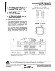
SCLS007D − MARCH 1984 − REVISED AUGUST 2003
2
POST OFFICE BOX 655303 • DALLAS, TEXAS 75265
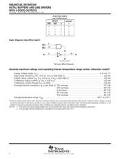
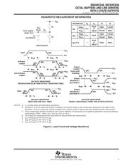
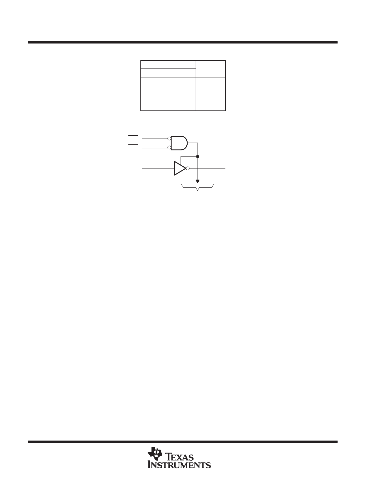
FUNCTION TABLE
(each buffer/driver)
INPUTS
OUTPUT
OE1 OE2 A
OUTPUT
Y
L L L H
L LH L
H XX Z
X H X Z
logic diagram (positive logic)
OE1
OE2
To Seven Other Channels
A1
Y1
1
19
218
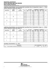
absolute maximum ratings over operating free-air temperature range (unless otherwise noted)
†
Supply voltage range, V
CC
−0.5 V to 7 V. . . . . . . . . . . . . . . . . . . . . . . . . . . . . . . . . . . . . . . . . . . . . . . . . . . . . . . . . .
Input clamp current, I
IK
(V
I
< 0 or V
I
> V
CC
) (see Note 1) ±20 mA. . . . . . . . . . . . . . . . . . . . . . . . . . . . . . . . . . . .
Output clamp current, I
OK
(V
O
< 0 or V
O
> V
CC
) (see Note 1) ±20 mA. . . . . . . . . . . . . . . . . . . . . . . . . . . . . . . .
Continuous output current, I
O
(V
O
= 0 to V
CC
) ±35 mA. . . . . . . . . . . . . . . . . . . . . . . . . . . . . . . . . . . . . . . . . . . . . .
Continuous current through V
CC
or GND ±70 mA. . . . . . . . . . . . . . . . . . . . . . . . . . . . . . . . . . . . . . . . . . . . . . . . . . .
Package thermal impedance, θ
JA
(see Note 2): DB package 70°C/W. . . . . . . . . . . . . . . . . . . . . . . . . . . . . . . . .
DW package 58°C/W. . . . . . . . . . . . . . . . . . . . . . . . . . . . . . . . .
N package 69°C/W. . . . . . . . . . . . . . . . . . . . . . . . . . . . . . . . . . .
NS package 60°C/W. . . . . . . . . . . . . . . . . . . . . . . . . . . . . . . . .
PW package 83°C/W. . . . . . . . . . . . . . . . . . . . . . . . . . . . . . . . .
Storage temperature range, T
stg
−65°C to 150°C. . . . . . . . . . . . . . . . . . . . . . . . . . . . . . . . . . . . . . . . . . . . . . . . . . .
†
Stresses beyond those listed under “absolute maximum ratings” may cause permanent damage to the device. These are stress ratings only, and
functional operation of the device at these or any other conditions beyond those indicated under “recommended operating conditions” is not
implied. Exposure to absolute-maximum-rated conditions for extended periods may affect device reliability.
NOTES: 1. The input and output voltage ratings may be exceeded if the input and output current ratings are observed.
2. The package thermal impedance is calculated in accordance with JESD 51-7.
器件 Datasheet 文档搜索
AiEMA 数据库涵盖高达 72,405,303 个元件的数据手册,每天更新 5,000 多个 PDF 文件
