Datasheet 搜索 > ON Semiconductor(安森美) > SN74LS165 数据手册 > SN74LS165 数据手册 3/8 页


¥ 0
SN74LS165 数据手册 - ON Semiconductor(安森美)
制造商:
ON Semiconductor(安森美)
描述:
小功率肖特基 LOW POWER SCHOTTKY
Pictures:
3D模型
符号图
焊盘图
引脚图
产品图
页面导航:
封装尺寸在P6P7P8
型号编码规则在P1P8
导航目录
SN74LS165数据手册
Page:
of 8 Go
若手册格式错乱,请下载阅览PDF原文件
SN74LS165
http://onsemi.com
3
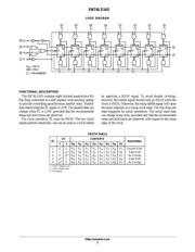
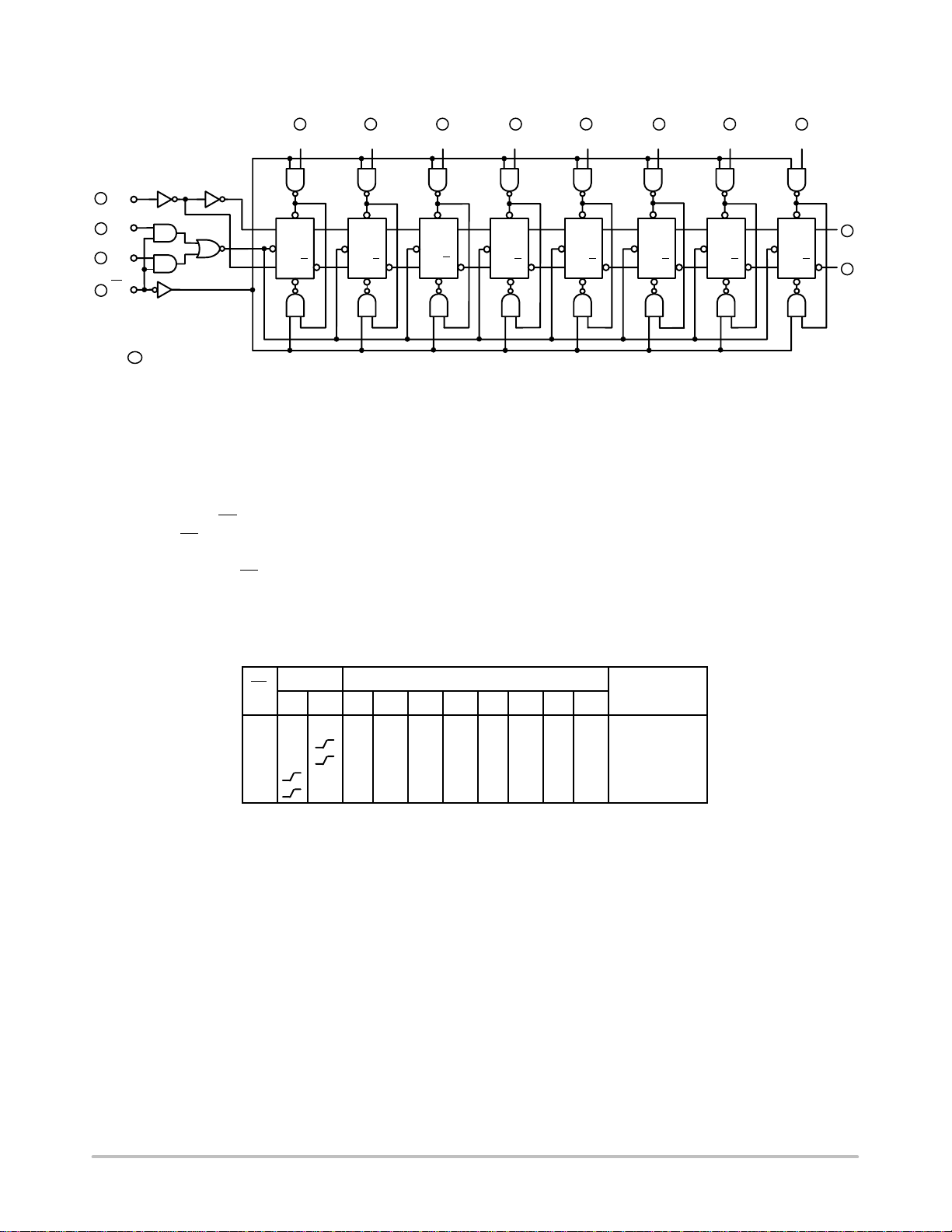
LOGIC DIAGRAM
PL
CP
1
P
4
P
6
P
5
P
7
CP
2
P
3
P
1
P
2
P
0
D
S
PRESET
S
CP
R
C
L
Q
0
Q
0
PRESET
S
CP
R
C
L
Q
1
Q
1
PRESET
S
CP
R
C
L
Q
2
Q
2
PRESET
S
CP
R
C
L
Q
3
Q
3
PRESET
S
CP
R
C
L
Q
4
Q
4
PRESET
S
CP
R
C
L
Q
5
Q
5
PRESET
S
CP
R
C
L
Q
6
Q
6
PRESET
S
CP
R
C
L
Q
7
Q
7
14
1
2
6
3 4 511 12
10
13
15
V
CC
= PIN 16
GND = PIN 8
= PIN NUMBERS
7
9
FUNCTIONAL DESCRIPTION
The SN74LS165 contains eight clocked master/slave RS
flip-flops connected as a shift register, with auxiliary gating
to provide overriding asynchronous parallel entry. Parallel
data enters when the PL signal is LOW. The parallel data can
change while PL is LOW, provided that the recommended
setup and hold times are observed.
For clock operation, PL
must be HIGH. The two clock
inputs perform identically; one can be used as a clock inhibit
by applying a HIGH signal. To avoid double clocking,
however, the inhibit signal should only go HIGH while the
clock is HIGH. Otherwise, the rising inhibit signal will cause
the same response as a rising clock edge. The flip-flops are
edge-triggered for serial operations. The serial input data
can change at any time, provided only that the recommended
setup and hold times are observed, with respect to the rising
edge of the clock.
TRUTH TABLE
PL
CP CONTENTS
RESPONSE
PL
1 2 Q
0
Q
1
Q
2
Q
3
Q
4
Q
5
Q
6
Q
7
RESPONSE
L X X P
0
P
1
P
2
P
3
P
4
P
5
P
6
P
7
Parallel Entry
H L D
S
Q
0
Q
1
Q
2
Q
3
Q
4
Q
5
Q
6
Right Shift
H H Q
0
Q
1
Q
2
Q
3
Q
4
Q
5
Q
6
Q
7
No Change
H L D
S
Q
0
Q
1
Q
2
Q
3
Q
4
Q
5
Q
6
Right Shift
H H Q
0
Q
1
Q
2
Q
3
Q
4
Q
5
Q
6
Q
7
No Change
H = HIGH Voltage Level
L = LOW Voltage Level
X = Immaterial
器件 Datasheet 文档搜索
AiEMA 数据库涵盖高达 72,405,303 个元件的数据手册,每天更新 5,000 多个 PDF 文件
