Datasheet 搜索 > 逻辑芯片 > TI(德州仪器) > SN74LV1T125DCKR 数据手册 > SN74LV1T125DCKR 数据手册 1/20 页
 器件3D模型
¥ 0.385
SN74LV1T125DCKR 数据手册 - TI(德州仪器)
制造商:
TI(德州仪器)
分类:
逻辑芯片
封装:
SC-70-5
描述:
SN74LV1T125DCKR 编带
Pictures:
3D模型
符号图
焊盘图
引脚图
产品图
页面导航:
导航目录
SN74LV1T125DCKR数据手册
Page:
of 20 Go
若手册格式错乱,请下载阅览PDF原文件
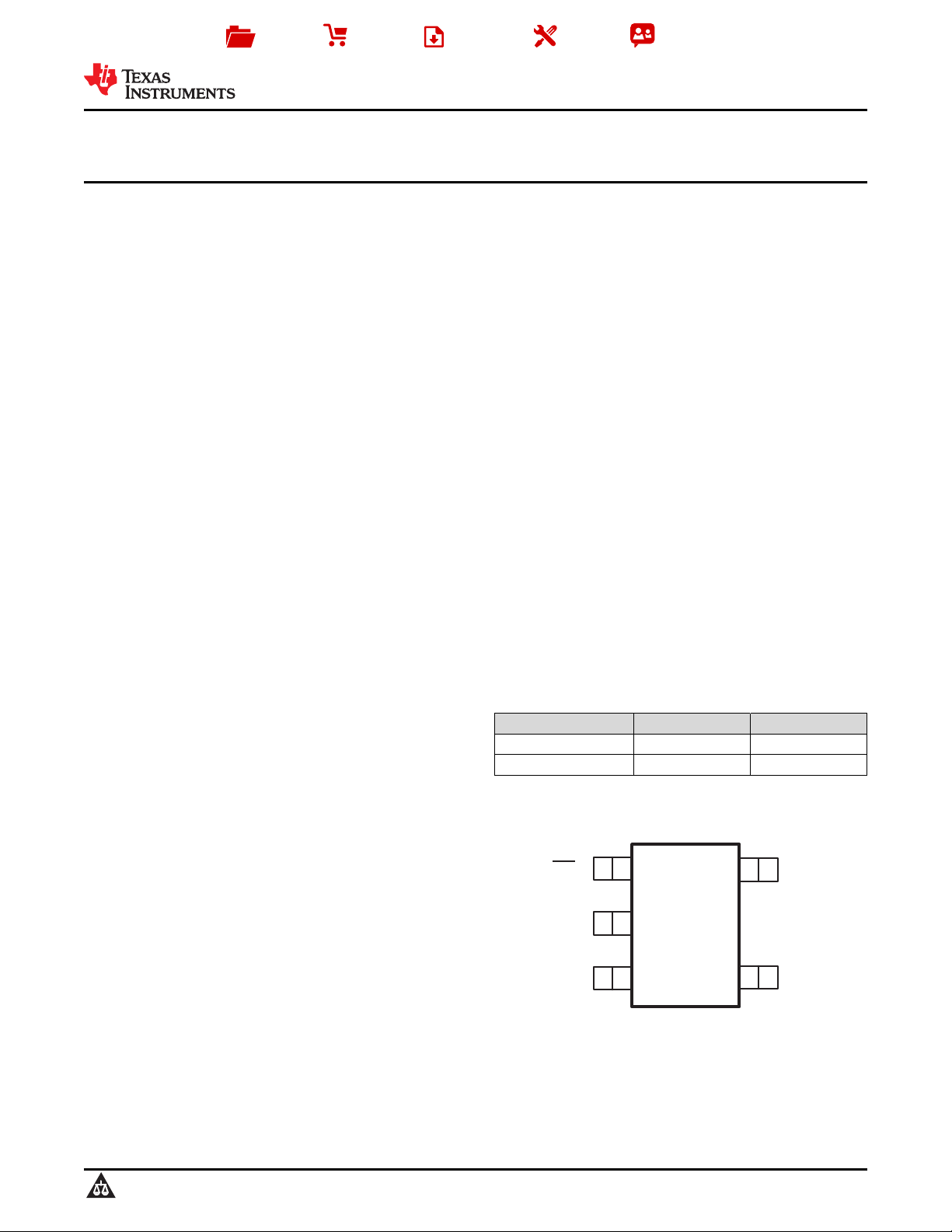
OE
A
GND
V
CC
Y
1
2
3
5
4
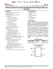
DCK or DBV PACKAGE
(TOP VIEW)
Product
Folder
Sample &
Buy
Technical
Documents
Tools &
Software
Support &
Community
SN74LV1T125
SCLS745A –DECEMBER 2013–REVISED FEBRUARY 2014
SN74LV1T125 Single Power Supply Single Buffer Gate with 3-State Output CMOS Logic
Level Shifter
1 Features 2 Applications
1
• Single-Supply Voltage Translator at
• Industrial controllers
5.0/3.3/2.5/1.8V V
CC
• Telecom
• Operating Range of 1.8V to 5.5V
• Portable applications
• Up Translation
• Servers
– 1.2V
(1)
to 1.8V at 1.8V V
CC • PC and notebooks
– 1.5V
(1)
to 2.5V at 2.5V V
CC
• Automotive
– 1.8V
(1)
to 3.3V at 3.3V V
CC
3 Description
– 3.3V to 5.0V at 5.0VV
CC
SN74LV1T125 is a low voltage CMOS gate logic that
• Down Translation
operates at a wider voltage range for industrial,
– 3.3V to 1.8V at 1.8V V
CC
portable, telecom, and automotive applications. The
– 3.3V to 2.5V at 2.5V V
CC
output level is referenced to the supply voltage and is
able to support 1.8V/2.5V/3.3V/5V CMOS levels.
– 5.0V to 3.3V at 3.3V V
CC
The input is designed with a lower threshold circuit to
• Logic Output is Referenced to V
CC
match 1.8V input logic at V
CC
= 3.3V and can be used
• Output Drive
in 1.8V to 3.3V level up translation. In addition, the
– 8.0mA Output Drive at 5.0V
5V tolerant input pins enable down translation (e.g.
– 7.0mA Output Drive at 3.3V
3.3V to 2.5V output at V
CC
= 2.5V). The wide V
CC
range of 1.8V to 5.5V allows generation of desired
– 3.0mA Output Drive at 1.8V
output levels to connect to controllers or processors.
• Characterized up to 50MHz at 3.3V V
CC
The SN74LV1T125 is designed with current-drive
• 5.0V Tolerance on Input Pins
capability of 8 mA to reduce line reflections,
• –40°C to 125°C Operating Temperature Range
overshoot, and undershoot caused by high-drive
• Latch-Up Performance Exceeds 250mA
outputs.
Per JESD 17
Device Information
• ESD Performance Tested Per JESD 22
ORDER NUMBER PACKAGE BODY SIZE
– 2000-V Human-Body Model
SN74LV1T125DBVR SOT-23 (5) 2,90mm x 1,60mm
(A114-B, Class II)
SN74LV1T125DCKR SC70 (5) 2,00mm x 1,25mm
– 200-V Machine Model (A115-A)
– 1000-V Charged-Device Model (C101)
• Supports Standard Logic Pinouts
• CMOS Output B Compatible with AUP1G and
LVC1G Families
(1)
Refer to the V
IH
/V
IL
and output drive for lower V
CC
condition
1
An IMPORTANT NOTICE at the end of this data sheet addresses availability, warranty, changes, use in safety-critical applications,
intellectual property matters and other important disclaimers. PRODUCTION DATA.
器件 Datasheet 文档搜索
AiEMA 数据库涵盖高达 72,405,303 个元件的数据手册,每天更新 5,000 多个 PDF 文件
