Datasheet 搜索 > 逻辑控制器 > TI(德州仪器) > SN74LVC139ADR 数据手册 > SN74LVC139ADR 数据手册 3/22 页
 器件3D模型
¥ 0.738
SN74LVC139ADR 数据手册 - TI(德州仪器)
制造商:
TI(德州仪器)
分类:
逻辑控制器
封装:
SOIC-16
描述:
74LVC Family Decoders/Multiplexers, Texas InstrumentsTexas Instruments range of Decoders, Multiplexers and De-multiplexers from the 74LVC Family of Low-voltage CMOS Logic ICs. The 74LVC Family use silicon gate CMOS technology and is designed to operate at 3.3V, allowing a significant reduction in power consumption when compared to 5V systems.Operating Voltage: 1.65 to 3.6V 5V tolerant inputs Compatibility: Input LVTTL/TTL, Output LVCMOS Latch-up performance exceeds 250 mA per JESD 17 ESD protection exceeds JESD 22 ### 74LVC 系列
Pictures:
3D模型
符号图
焊盘图
引脚图
产品图
页面导航:
导航目录
SN74LVC139ADR数据手册
Page:
of 22 Go
若手册格式错乱,请下载阅览PDF原文件
www.ti.com
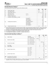
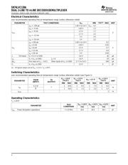
Absolute Maximum Ratings
(1)
Recommended Operating Conditions
(1)
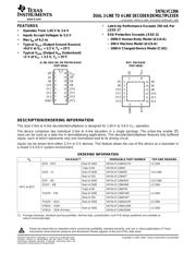
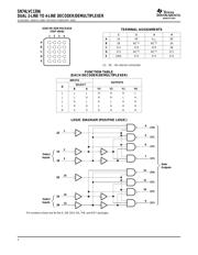
SN74LVC139A
DUAL 2-LINE TO 4-LINE DECODER/DEMULTIPLEXER
SCAS341O – MARCH 1994 – REVISED FEBRUARY 2005
over operating free-air temperature range (unless otherwise noted)
MIN MAX UNIT
V
CC
Supply voltage range –0.5 6.5 V
V
I
Input voltage range
(2)
–0.5 6.5 V
V
O
Output voltage range
(2) (3)
–0.5 V
CC
+ 0.5 V
I
IK
Input clamp current V
I
< 0 –50 mA
I
OK
Output clamp current V
O
< 0 –50 mA
I
O
Continuous output current ± 50 mA
Continuous current through V
CC
or GND ± 100 mA
D package
(4)
73
DB package
(4)
82
DGV package
(4)
120
θ
JA
Package thermal impedance GQN/ZQN package
(4)
78 ° C/W
NS package
(4)
64
PW package
(4)
108
RGY package
(5)
39
T
stg
Storage temperature range –65 150 ° C
(1) Stresses beyond those listed under "absolute maximum ratings" may cause permanent damage to the device. These are stress ratings
only, and functional operation of the device at these or any other conditions beyond those indicated under "recommended operating
conditions" is not implied. Exposure to absolute-maximum-rated conditions for extended periods may affect device reliability.
(2) The input and output negative-voltage ratings may be exceeded if the input and output current ratings are observed.
(3) The value of V
CC
is provided in the recommended operating conditions table.
(4) The package thermal impedance is calculated in accordance with JESD 51-7.
(5) The package thermal impedance is calculated in accordance with JESD 51-5.
MIN MAX UNIT
Operating 1.65 3.6
V
CC
Supply voltage V
Data retention only 1.5
V
CC
= 1.65 V to 1.95 V 0.65 × V
CC
V
IH
High-level input voltage V
CC
= 2.3 V to 2.7 V 1.7 V
V
CC
= 2.7 V to 3.6 V 2
V
CC
= 1.65 V to 1.95 V 0.35 × V
CC
V
IL
Low-level input voltage V
CC
= 2.3 V to 2.7 V 0.7 V
V
CC
= 2.7 V to 3.6 V 0.8
V
I
Input voltage 0 5.5 V
V
O
Output voltage 0 V
CC
V
V
CC
= 1.65 V –4
V
CC
= 2.3 V –8
I
OH
High-level output current mA
V
CC
= 2.7 V –12
V
CC
= 3 V –24
V
CC
= 1.65 V 4
V
CC
= 2.3 V 8
I
OL
Low-level output current mA
V
CC
= 2.7 V 12
V
CC
= 3 V 24
∆ t/ ∆ v Input transition rise or fall rate 10 ns/V
T
A
Operating free-air temperature –40 85 ° C
(1) All unused inputs of the device must be held at V
CC
or GND to ensure proper device operation. Refer to the TI application report,
Implications of Slow or Floating CMOS Inputs, literature number SCBA004.
3
器件 Datasheet 文档搜索
AiEMA 数据库涵盖高达 72,405,303 个元件的数据手册,每天更新 5,000 多个 PDF 文件
