Datasheet 搜索 > 逻辑芯片 > TI(德州仪器) > SN74LVC1G08QDCKRQ1 数据手册 > SN74LVC1G08QDCKRQ1 数据手册 1/19 页
 器件3D模型
¥ 0.602
SN74LVC1G08QDCKRQ1 数据手册 - TI(德州仪器)
制造商:
TI(德州仪器)
分类:
逻辑芯片
封装:
SC-70-5
描述:
74LVC1G 系列,Texas Instruments低电压 CMOS 逻辑 单门封装 工作电压:1.65 - 5.5 兼容性:输入 LVTTL/TTL、输出 LVCMOS 按 JESD 78 II 级标准,闩锁效应性能超过 100 mA。 ESD 保护超乎 JESD 22 标准 ### 74LVC 系列
Pictures:
3D模型
符号图
焊盘图
引脚图
产品图
页面导航:
导航目录
SN74LVC1G08QDCKRQ1数据手册
Page:
of 19 Go
若手册格式错乱,请下载阅览PDF原文件

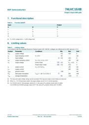
1. General description
The 74LVC1G08 provides one 2-input AND function.
Inputs can be driven from either 3.3 V or 5 V devices. This feature allows the use of these
devices as translators in mixed 3.3 V and 5 V applications.
Schmitt trigger action at all inputs makes the circuit tolerant of slower input rise and fall
time.
This device is fully specified for partial power-down applications using I
OFF
.
The I
OFF
circuitry disables the output, preventing the damaging backflow current through
the device when it is powered down.
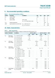
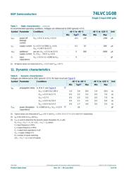
2. Features and benefits
Wide supply voltage range from 1.65 V to 5.5 V
High noise immunity
Complies with JEDEC standard:
JESD8-7 (1.65 V to 1.95 V)
JESD8-5 (2.3 V to 2.7 V)
JESD8-B/JESD36 (2.7 V to 3.6 V)
24 mA output drive (V
CC
=3.0V)
CMOS low power consumption
Latch-up performance 250 mA
Direct interface with TTL levels
Inputs accept voltages up to 5 V
ESD protection:
HBM JESD22-A114F exceeds 2000 V
MM JESD22-A115-A exceeds 200 V
Multiple package options
Specified from 40 C to +85 C and 40 C to +125 C
74LVC1G08
Single 2-input AND gate
Rev. 10 — 29 June 2012 Product data sheet
器件 Datasheet 文档搜索
AiEMA 数据库涵盖高达 72,405,303 个元件的数据手册,每天更新 5,000 多个 PDF 文件
