Datasheet 搜索 > TI(德州仪器) > SN74LVC1G139DCT 数据手册 > SN74LVC1G139DCT 数据手册 5/22 页


¥ 0
SN74LVC1G139DCT 数据手册 - TI(德州仪器)
制造商:
TI(德州仪器)
Pictures:
3D模型
符号图
焊盘图
引脚图
产品图
页面导航:
引脚图在P3Hot
典型应用电路图在P10P11
原理图在P1P9
封装尺寸在P13P15P16
标记信息在P13P14
封装信息在P12P13P14P15P16
技术参数、封装参数在P3
应用领域在P1P22
电气规格在P5
导航目录
SN74LVC1G139DCT数据手册
Page:
of 22 Go
若手册格式错乱,请下载阅览PDF原文件
SN74LVC1G139
www.ti.com
SCES602D –AUGUST 2004–REVISED AUGUST 2015
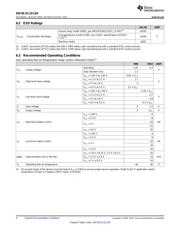
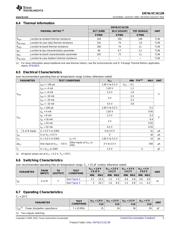
6.4 Thermal Information
SN74LVC1G139
THERMAL METRIC
(1)
DCT (SM8) DCU (VSSOP) YZP (DSBGA) UNIT
8 PINS 8 PINS 8 PINS
R
θJA
Junction-to-ambient thermal resistance 194 195 106 °C/W
R
θJC(top)
Junction-to-case (top) thermal resistance 124 74 1.6 °C/W
R
θJB
Junction-to-board thermal resistance 106 74 11 °C/W
ψ
JT
Junction-to-top characterization parameter 48 6.7 3.1 °C/W
ψ
JB
Junction-to-board characterization parameter 105 73 11 °C/W
R
θJC(bot)
Junction-to-case (bottom) thermal resistance — — — °C/W
(1) For more information about traditional and new thermal metrics, see the Semiconductor and IC Package Thermal Metrics application
report, SPRA953.
6.5 Electrical Characteristics
over recommended operating free-air temperature range (unless otherwise noted)
PARAMETER TEST CONDITIONS V
CC
MIN TYP
(1)
MAX UNIT
I
OH
= –100 µA 1.65 V to 5.5 V V
CC
– 0.1
I
OH
= –4 mA 1.65 V 1.2
I
OH
= –8 mA 2.3 V 1.9
V
OH
V
I
OH
= –16 mA 2.4
3 V
I
OH
= –24 mA 2.3
I
OH
= –32 mA 4.5 V 3.8
I
OL
= 100 µA 1.65 V to 5.5 V 0.1
I
OL
= 4 mA 1.65 V 0.45
I
OL
= 8 mA 2.3 V 0.3
V
OL
V
I
OL
= 16 mA 0.4
3 V
I
OL
= 24 mA 0.55
I
OL
= 32 mA 4.5 V 0.55
I
I
A or B inputs V
I
= 5.5 V or GND 0 to 5.5 V ±1 µA
I
off
V
I
or V
O
= 5.5 V 0 ±5 µA
I
CC
V
I
= 5.5 V or GND, I
O
= 0 1.65 V to 5.5 V 10 µA
Other inputs at V
CC
or
ΔI
CC
One input at V
CC
– 0.6 V, 3 V to 5.5 V 500 µA
GND
C
i
V
I
= V
CC
or GND 3.3 V 4 pF
(1) All typical values are at V
CC
= 3.3 V, T
A
= 25°C.
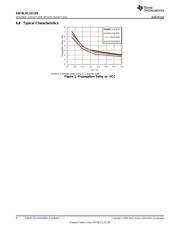
6.6 Switching Characteristics
over recommended operating free-air temperature range, C
L
= 15 pF (unless otherwise noted)
V
CC
= 1.8 V V
CC
= 2.5 V V
CC
= 3.3 V V
CC
= 5 V
FROM TO TEST
± 0.15 V ± 0.2 V ± 0.3 V ± 0.5 V
PARAMETER UNIT
(INPUT) (OUTPUT) CONDITIONS
MIN MAX MIN MAX MIN MAX MIN MAX
See Figure 2 2.7 15.3 1.5 7.5 0.9 4.9 0.8 3.6
t
pd
A or B Y ns
See Figure 3 3 16.7 1.6 8.2 1.2 5.9 1.1 4.2
6.7 Operating Characteristics
T
A
= 25°C
V
CC
= 1.8 V V
CC
= 2.5 V V
CC
= 3.3 V V
CC
= 5 V
TEST
PARAMETER UNIT
CONDITIONS
TYP TYP TYP TYP
C
pd
(1)
Power dissipation capacitance f = 10 MHz 31 34 36 39 pF
(1) Two outputs switching.
Copyright © 2004–2015, Texas Instruments Incorporated Submit Documentation Feedback 5
Product Folder Links: SN74LVC1G139
器件 Datasheet 文档搜索
AiEMA 数据库涵盖高达 72,405,303 个元件的数据手册,每天更新 5,000 多个 PDF 文件
