Datasheet 搜索 > 逻辑控制器 > TI(德州仪器) > SN74LVC1G17QDBVRQ1 数据手册 > SN74LVC1G17QDBVRQ1 数据手册 1/14 页


¥ 0.713
SN74LVC1G17QDBVRQ1 数据手册 - TI(德州仪器)
制造商:
TI(德州仪器)
分类:
逻辑控制器
封装:
SOT-23-5
描述:
单施密特触发缓冲器 SINGLE SCHMITT-TRIGGER BUFFER
Pictures:
3D模型
符号图
焊盘图
引脚图
产品图
页面导航:
封装尺寸在P6P8P9
标记信息在P6
封装信息在P6P7P8P9
应用领域在P7P14
导航目录
SN74LVC1G17QDBVRQ1数据手册
Page:
of 14 Go
若手册格式错乱,请下载阅览PDF原文件
1
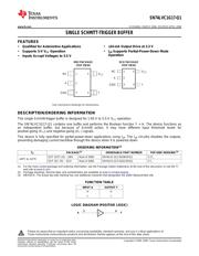
FEATURES
3
2
4
51
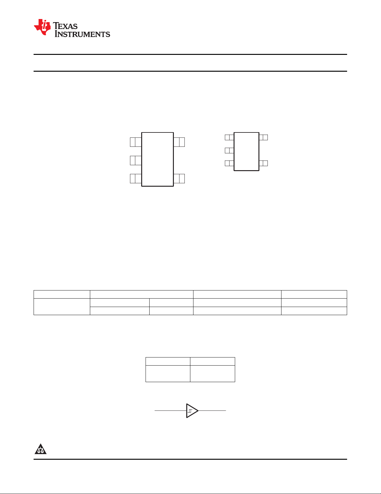
NC V
CC
Y
A
GND
DBV PACKAGE
(TOP VIEW)
DCK PACKAGE
(TOP VIEW)
3
2
4
51
NC V
CC
Y
A
GND
See mechanical drawings for dimensions.
DESCRIPTION/ORDERING INFORMATION
A Y
2 4
SN74LVC1G17-Q1
www.ti.com
........................................................................................................................................................ SCES663A – MARCH 2006 – REVISED APRIL 2008
SINGLE SCHMITT-TRIGGER BUFFER
• Qualified for Automotive Applications • ± 24-mA Output Drive at 3.3 V
• Supports 5-V V
CC
Operation • I
off
Supports Partial-Power-Down Mode
Operation
• Inputs Accept Voltages to 5.5 V
This single Schmitt-trigger buffer is designed for 1.65-V to 5.5-V V
CC
operation.
The SN74LVC1G17-Q1 contains one buffer and performs the Boolean function Y = A. The device functions as
an independent buffer, but because of Schmitt action, it may have different input threshold levels for
positive-going (V
T+
) and negative-going (V
T –
) signals.
This device is fully specified for partial-power-down applications using I
off
. The I
off
circuitry disables the outputs,
preventing damaging current backflow through the device when it is powered down.
ORDERING INFORMATION
(1)
T
A
PACKAGE
(2)
ORDERABLE PART NUMBER TOP-SIDE MARKING
(3)
SOT (SOT-23) – DBV Reel of 3000 SN74LVC1G17QDBVRQ1 C17_
– 40 ° C to 125 ° C
SOT (SC-70) – DCK Reel of 3000 SN74LVC1G17QDCKRQ1 C7_
(1) For the most current package and ordering information, see the Package Option Addendum at the end of this document, or see the TI
web site at www.ti.com .
(2) Package drawings, thermal data, and symbolization are available at www.ti.com/packaging .
(3) DBV/DCK: The actual top-side marking has one additional character that designates the wafer fab/assembly site.
FUNCTION TABLE
INPUT A OUTPUT Y
H H
L L
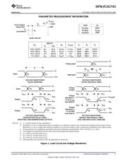
LOGIC DIAGRAM (POSITIVE LOGIC)
1
Please be aware that an important notice concerning availability, standard warranty, and use in critical applications of
Texas Instruments semiconductor products and disclaimers thereto appears at the end of this data sheet.
PRODUCTION DATA information is current as of publication date.
Copyright © 2006 – 2008, Texas Instruments Incorporated
Products conform to specifications per the terms of the Texas
Instruments standard warranty. Production processing does not
necessarily include testing of all parameters.
器件 Datasheet 文档搜索
AiEMA 数据库涵盖高达 72,405,303 个元件的数据手册,每天更新 5,000 多个 PDF 文件
