Datasheet 搜索 > 逻辑控制器 > TI(德州仪器) > SN74LVC1G18DBVR 数据手册 > SN74LVC1G18DBVR 数据手册 2/23 页

¥ 0.501
SN74LVC1G18DBVR 数据手册 - TI(德州仪器)
制造商:
TI(德州仪器)
分类:
逻辑控制器
封装:
SOT-23-6
描述:
TEXAS INSTRUMENTS SN74LVC1G18DBVR 芯片, 多路复用器/分离器, 单路, 1通道, SOT-23-6
Pictures:
3D模型
符号图
焊盘图
引脚图
产品图
页面导航:
典型应用电路图在P2
封装尺寸在P2P8P10P11P20
焊盘布局在P21
型号编码规则在P1P2
标记信息在P2P8P9
封装信息在P8P9P10P11
技术参数、封装参数在P2
应用领域在P23
电气规格在P4
导航目录
SN74LVC1G18DBVR数据手册
Page:
of 23 Go
若手册格式错乱,请下载阅览PDF原文件
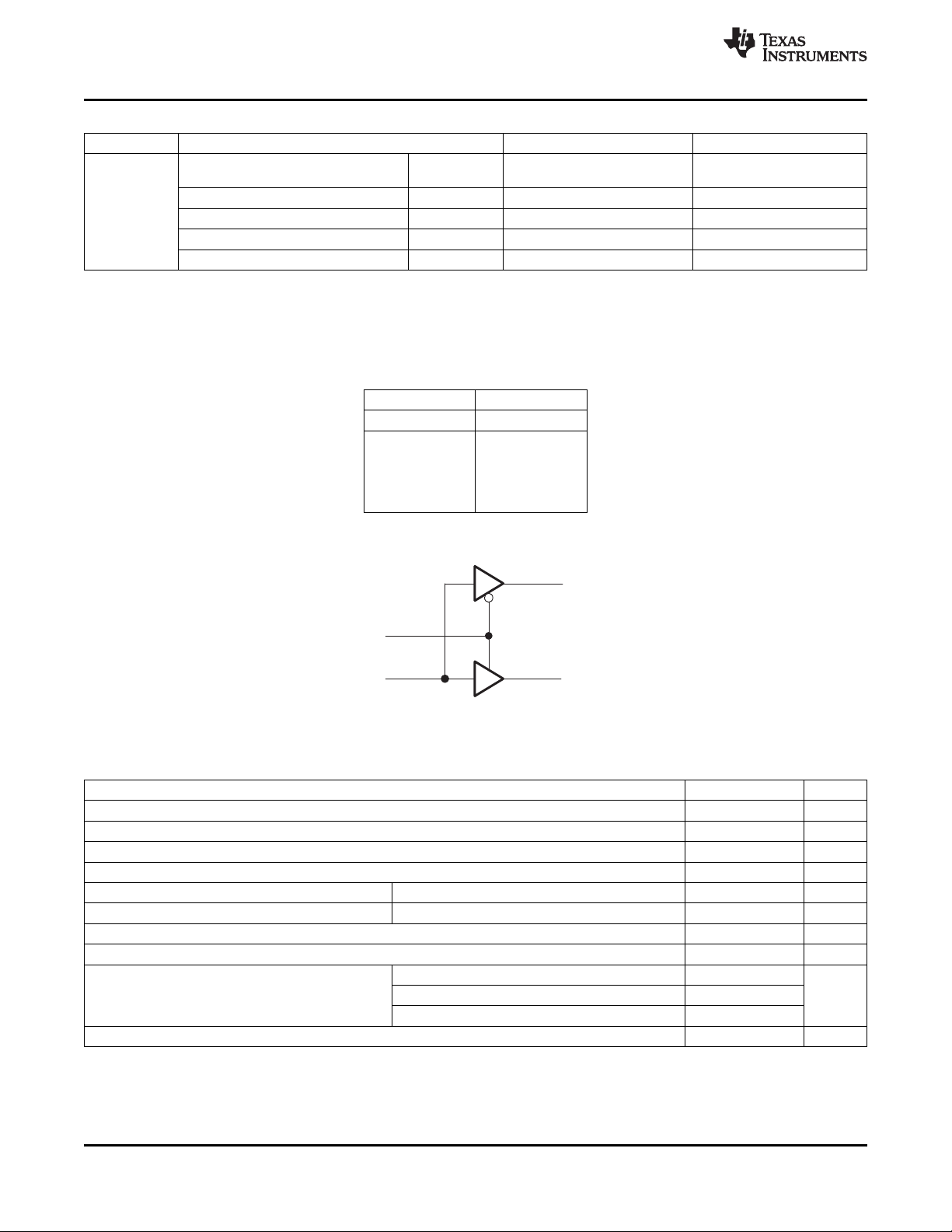
A Y1
3 4
S
1
Y0
6
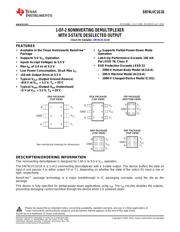
SN74LVC1G18
SCES406K –JULY 2002–REVISED JULY 2012
www.ti.com
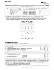
ORDERING INFORMATION
T
A
PACKAGE
(1)
ORDERABLE PART NUMBER TOP-SIDE MARKING
(2)
NanoFree™ – WCSP (DSBGA)
Reel of 3000 SN74LVC1G18YZPR _ _ _CJ_
0.23-mm Large Bump – YZP (Pb-free)
SOT (SOT-23) – DBV Reel of 3000 SN74LVC1G18DBVR C18_
–40°C to 85°C
SOT (SC-70) – DCK Reel of 3000 SN74LVC1G18DCKR CJ_
QFN – DRY Reel of 5000 SN74LVC1G18DRYR CJ
µQFN – DSF Reel of 5000 SN74LVC1G18DSFR CJ
(1) Package drawings, standard packing quantities, thermal data, symbolization, and PCB design guidelines are available at
www.ti.com/sc/package.
(2) DBV/DCK: The actual top-side marking has one additional character that designates the assembly/test site.
YZP: The actual top-side marking has three preceding characters to denote year, month, and sequence code, and one following
character to designate the assembly/test site. Pin 1 identifier indicates solder-bump composition (1 = SnPb, • = Pb-free).
Table 1. FUNCTION TABLE
INPUTS OUTPUTS
S A Y0 Y1
L L L Z
L H H Z
H L Z L
H H Z H
LOGIC DIAGRAM (POSITIVE LOGIC)
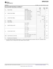
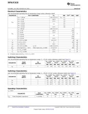
Absolute Maximum Ratings
(1)
over operating free-air temperature range (unless otherwise noted)
MIN MAX UNIT
V
CC
Supply voltage range –0.5 6.5 V
V
I
Input voltage range
(2)
–0.5 6.5 V
V
O
Voltage range applied to any output in the high-impedance or power-off state
(2)
–0.5 6.5 V
V
O
Voltage range applied to any output in the high or low state
(2) (3)
–0.5 V
CC
+ 0.5 V
I
IK
Input clamp current V
I
< 0 –50 mA
I
OK
Output clamp current V
O
< 0 –50 mA
I
O
Continuous output current ±50 mA
Continuous current through V
CC
or GND ±100 mA
DBV package 165
θ
JA
Package thermal impedance
(4)
DCK package 259 °C/W
YZP package 123
T
stg
Storage temperature range –65 150 °C
(1) Stresses beyond those listed under "absolute maximum ratings" may cause permanent damage to the device. These are stress ratings
only, and functional operation of the device at these or any other conditions beyond those indicated under "recommended operating
conditions" is not implied. Exposure to absolute-maximum-rated conditions for extended periods may affect device reliability.
(2) The input negative-voltage and output voltage ratings may be exceeded if the input and output current ratings are observed.
(3) The value of V
CC
is provided in the recommended operating conditions table.
(4) The package thermal impedance is calculated in accordance with JESD 51-7.
2 Submit Documentation Feedback Copyright © 2002–2012, Texas Instruments Incorporated
Product Folder Link(s): SN74LVC1G18
器件 Datasheet 文档搜索
AiEMA 数据库涵盖高达 72,405,303 个元件的数据手册,每天更新 5,000 多个 PDF 文件
