Datasheet 搜索 > 触发器 > TI(德州仪器) > SN74LVC1G74RSE2 数据手册 > SN74LVC1G74RSE2 数据手册 1/21 页
 器件3D模型
¥ 2.365
SN74LVC1G74RSE2 数据手册 - TI(德州仪器)
制造商:
TI(德州仪器)
分类:
触发器
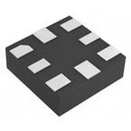
封装:
UQFN-8
描述:
具有清零和预置端的单路正边沿触发式 D 型触发器 8-UQFN -40 to 125
Pictures:
3D模型
符号图
焊盘图
引脚图
产品图
页面导航:
导航目录
SN74LVC1G74RSE2数据手册
Page:
of 21 Go
若手册格式错乱,请下载阅览PDF原文件
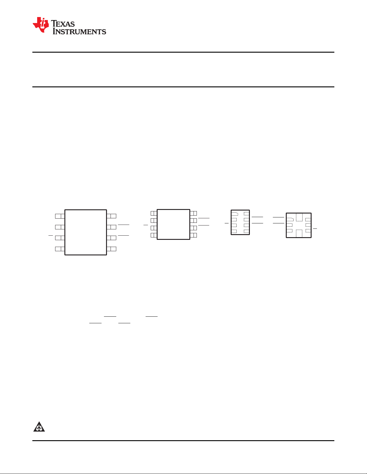
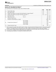
DCT PACKAGE
(TOP VIEW)
CLK
1
8
V
CC
D
2 7
PRE
Q
3 6
CLR
DCU PACKAGE
(TOP VIEW)
CLK
1 8
V
CC
D
2 7
PRE
Q
3 6
CLR
GND
4 5
Q
GND
4
5
Q
See mechanical drawings for dimensions
.
DQE PACKAGE
(TOP VIEW)
CLK
1
8
V
CC
D
Q
GND
2 7
3 6
4 5
PRE
CLR
Q
RSE PACKAGE
(TOP VIEW)
CLK
1
8
V
CC
D
Q
GND
2
7
3
6
4
5
PRE
CLR
Q
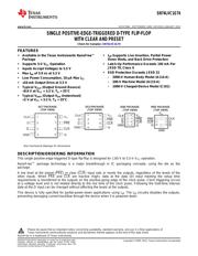
SN74LVC1G74
www.ti.com
SCES794D –SEPTEMBER 2009–REVISED JANUARY 2013
SINGLE POSITIVE-EDGE-TRIGGERED D-TYPE FLIP-FLOP
WITH CLEAR AND PRESET
Check for Samples: SN74LVC1G74
1
FEATURES
2
• Available in the Texas Instruments NanoFree™
• I
off
Supports Live Insertion, Partial Power
Package Down Mode, and Back Drive Protection
• Supports 5-V V
CC
Operation • Latch-Up Performance Exceeds 100 mA Per
JESD 78, Class II
• Inputs Accept Voltages to 5.5 V
• ESD Protection Exceeds JESD 22
• Max t
pd
of 5.9 ns at 3.3 V
– 2000-V Human-Body Model (A114-A)
• Low Power Consumption, 10-μA Max I
CC
– 200-V Machine Model (A115-A)
• ±24-mA Output Drive at 3.3 V
– 1000-V Charged-Device Model (C101)
• Typical V
OLP
(Output Ground Bounce)
<0.8 V at V
CC
= 3.3 V, T
A
= 25°C
• Typical V
OHV
(Output V
OH
Undershoot)
>2 V at V
CC
= 3.3 V, T
A
= 25°C
DESCRIPTION/ORDERING INFORMATION
This single positive-edge-triggered D-type flip-flop is designed for 1.65-V to 5.5-V V
CC
operation.
NanoFree™ package technology is a major breakthrough in IC packaging concepts, using the die as the
package.
A low level at the preset (PRE) or clear (CLR) input sets or resets the outputs, regardless of the levels of the
other inputs. When PRE and CLR are inactive (high), data at the data (D) input meeting the setup time
requirements is transferred to the outputs on the positive-going edge of the clock pulse. Clock triggering occurs
at a voltage level and is not related directly to the rise time of the clock pulse. Following the hold-time interval,
data at the D input can be changed without affecting the levels at the outputs.
This device is fully specified for partial-power-down applications using I
off
. The I
off
circuitry disables the outputs,
preventing damaging current backflow through the device when it is powered down.
1
Please be aware that an important notice concerning availability, standard warranty, and use in critical applications of
Texas Instruments semiconductor products and disclaimers thereto appears at the end of this data sheet.
2NanoFree is a trademark of Texas Instruments.
PRODUCTION DATA information is current as of publication date.
Copyright © 2009–2013, Texas Instruments Incorporated
Products conform to specifications per the terms of the Texas
Instruments standard warranty. Production processing does not
necessarily include testing of all parameters.
器件 Datasheet 文档搜索
AiEMA 数据库涵盖高达 72,405,303 个元件的数据手册,每天更新 5,000 多个 PDF 文件
