Datasheet 搜索 > TI(德州仪器) > SN74LVC2G04 数据手册 > SN74LVC2G04 数据手册 8/26 页

¥ 0
SN74LVC2G04 数据手册 - TI(德州仪器)
制造商:
TI(德州仪器)
描述:
双反向器
Pictures:
3D模型
符号图
焊盘图
引脚图
产品图
页面导航:
引脚图在P3Hot
典型应用电路图在P1P9P10
原理图在P8P9
封装尺寸在P13P15P16P23
焊盘布局在P24
标记信息在P13P14
封装信息在P3P12P13P14P15P16
技术参数、封装参数在P4P9
应用领域在P1P14P26
电气规格在P5
型号编号列表在P9


导航目录
SN74LVC2G04数据手册
Page:
of 26 Go
若手册格式错乱,请下载阅览PDF原文件
1A 1Y
1 6
2A 2Y
3 4
SN74LVC2G04
SCES195N –APRIL 1999–REVISED AUGUST 2015
www.ti.com
8 Detailed Description
8.1 Overview
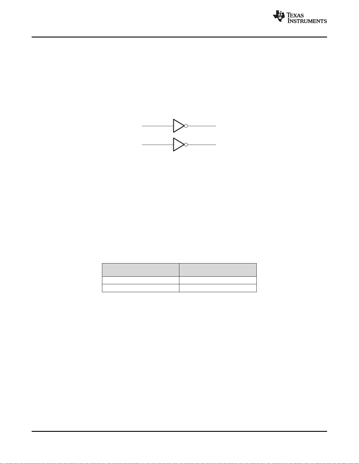
The SN74LVC2G04 contains two identical inverters that operate from 1.65-V to 5.5-V V
CC
. Each inverter has a
balanced output capable of outputting 32 mA at V
CC
= 4.5 V. The overvoltage tolerant inputs allow for down-
translation of up to 6.5 V, and the partial power-off feature ensures that the inputs and outputs can be any value
from –0.5 V to 6.5 V when V
CC
is 0 V
8.2 Functional Block Diagram
8.3 Feature Description
NanoFree package technology is a major breakthrough in IC packaging concepts, using the die as the package.
This device supports 5-V V
CC
operation and up to 5.5-V inputs. It has a low propagation delay of only 4.1 ns at
3.3 V.
Power consumption is low with only 10-μA Max I
CC
. Balanced drive output at 3.3 V can put out ±24-mA.
Typical output ground bounce is less than 0.8 V at 3.3-V V
CC
and typical output undershoot is greater than 2 V at
3.3-V V
CC
.
This device supports partial-power-down mode operation.
8.4 Device Functional Modes
Table 1 lists the functional modes of the SN74LVC2G04.
Table 1. Function Table (Each Inverter)
INPUT OUTPUT
A Y
H L
L H
8 Submit Documentation Feedback Copyright © 1999–2015, Texas Instruments Incorporated
Product Folder Links: SN74LVC2G04
器件 Datasheet 文档搜索
AiEMA 数据库涵盖高达 72,405,303 个元件的数据手册,每天更新 5,000 多个 PDF 文件
