Datasheet 搜索 > 逻辑芯片 > TI(德州仪器) > SN74LVC2G08DCUT 数据手册 > SN74LVC2G08DCUT 数据手册 2/16 页
 器件3D模型
¥ 3.363
SN74LVC2G08DCUT 数据手册 - TI(德州仪器)
制造商:
TI(德州仪器)
分类:
逻辑芯片
封装:
VSSOP-8
描述:
TEXAS INSTRUMENTS SN74LVC2G08DCUT 逻辑芯片, 正与门, 双路, 2输入, 8VSSOP
Pictures:
3D模型
符号图
焊盘图
引脚图
产品图
页面导航:
导航目录
SN74LVC2G08DCUT数据手册
Page:
of 16 Go
若手册格式错乱,请下载阅览PDF原文件
1
2
7
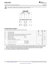
1A
1B
1Y
5
6
3
2A
2B
2Y
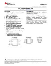
SN74LVC2G08
SCES198M –APRIL 1999–REVISED NOVEMBER 2013
www.ti.com
These devices have limited built-in ESD protection. The leads should be shorted together or the device placed in conductive foam
during storage or handling to prevent electrostatic damage to the MOS gates.
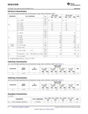
Function Fable
(Each Gate)
INPUTS
OUTPUT
Y
A B
H H H
L X L
X L L
Logic Diagram (Positive Logic)
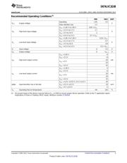
Absolute Maximum Ratings
(1)
over operating free-air temperature range (unless otherwise noted)
MIN MAX UNIT
V
CC
Supply voltage range –0.5 6.5 V
V
I
Input voltage range
(2)
–0.5 6.5 V
V
O
Voltage range applied to any output in the high-impedance or power-off state
(2)
–0.5 6.5 V
V
O
Voltage range applied to any output in the high or low state
(2)(3)
–0.5 V
CC
+ 0.5 V
I
IK
Input clamp current V
I
< 0 –50 mA
I
OK
Output clamp current V
O
< 0 –50 mA
I
O
Continuous output current ±50 mA
Continuous current through V
CC
or GND ±100 mA
DCT package 220
θ
JA
Package thermal impedance
(4)
DCU package 227 °C/W
YZP package 102
T
stg
Storage temperature range –65 150 °C
(1) Stresses beyond those listed under "absolute maximum ratings" may cause permanent damage to the device. These are stress ratings
only, and functional operation of the device at these or any other conditions beyond those indicated under "recommended operating
conditions" is not implied. Exposure to absolute-maximum-rated conditions for extended periods may affect device reliability.
(2) The input negative-voltage and output voltage ratings may be exceeded if the input and output current ratings are observed.
(3) The value of V
CC
is provided in the recommended operating conditions table.
(4) The package thermal impedance is calculated in accordance with JESD 51-7.
2 Submit Documentation Feedback Copyright © 1999–2013, Texas Instruments Incorporated
Product Folder Links: SN74LVC2G08
器件 Datasheet 文档搜索
AiEMA 数据库涵盖高达 72,405,303 个元件的数据手册,每天更新 5,000 多个 PDF 文件
